Unlock instant, AI-driven research and patent intelligence for your innovation.

Semiconductor heterostructure and method of fabrication thereof

Active Publication Date: 2016-10-18
BROLIS SENSOR TECHONOLOGY UAB
View PDF4 Cites 1 Cited by
  • Summary
  • Abstract
  • Description
  • Claims
  • Application Information

AI Technical Summary

Benefits of technology

This approach improves the crystalline quality, reduces defect creation, and enhances the performance of semiconductor devices by minimizing intermixing and interface degradation, leading to improved electrical and optical properties, including increased channel mobility and reduced leakage currents.

Problems solved by technology

Typically, heterostructures in binary, ternary, quaternary and quinternary system are grown under group-V-rich conditions, because group-III-rich conditions have been experiences to be disadvantageous due to droplet formation and the like.

Method used


Image

  • Semiconductor heterostructure and method of fabrication thereof
  • Semiconductor heterostructure and method of fabrication thereof
  • Semiconductor heterostructure and method of fabrication thereof

Examples


Embodiment Construction

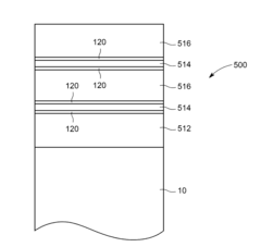
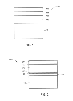
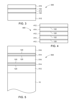
[0016]Reference will now be made in detail to the various embodiments of the invention, one or more examples of which are illustrated in the figures. Within the following description of the drawings, the same reference numbers refer to same components. Generally, only the differences with respect to individual embodiments are described. Each example is provided by way of explanation of the invention and is not meant as a limitation of the invention. Further, features illustrated or described as part of one embodiment can be used on or in conjunction with other embodiments to yield yet a further embodiment. It is intended that the description includes such modifications and variations.

[0017]Embodiments described herein refer to heterostructures. Accordingly, parts of e.g. a light emitting structure, such as a laser, a LED, a SLED, etc., are provided, wherein the heterostructures and devices include a compound semiconductor layer-stack. Typically, the formation of a heterostructure in...


PUM


Abstract

A III-V compound semiconductor heterostructure grown on a substrate is described. The heterostructure includes a first semiconductor layer, wherein the first layer semiconductor layer is a compound semiconductor layer with (III) (V), wherein (III) represents one or more group-III elements and (V) represents one or more group-V elements, an intermediate layer on the first semiconductor layer, wherein the intermediate layer is a compound semiconductor layer with (III)x>1(V)2-x, and wherein the intermediate layer has a thickness of 10 monolayers or below, and a second semiconductor layer, wherein the first layer semiconductor layer is a compound semiconductor layer with (III)1(V)1.

Description

TECHNICAL FIELD OF THE INVENTION[0001]Embodiments of the present invention relate to semiconductor heterostructures for electronic and optoelectronic devices. Embodiments of the present invention particularly relate to III-V-antimonide-heterostructures, and specifically to a III-V-compound semiconductor heterostructure.BACKGROUND OF THE INVENTION[0002]The demand for electronic devices and optoelectronic devices for the infrared range can be met by semiconductor heterostructures based on group-III antimonides. From III-V compound semiconductor materials, antimonides offer a comparable small band gap, from 1.65 eV of AlAsSb down to 0.2 eV of InSb. Therefore, devices based on III-V-antimonide-heterostructures are well-suited as emitters for optical data transmission, solar energy harvesting, gas sensing applications, medical applications, plastic welding, etc.[0003]For the fabrication of high-quality electronic and optoelectronic semiconductor devices, a precise control of the electron...

Claims


Application Information

Patent Timeline
Patent Type & Authority Patents(United States)
IPC IPC(8): H01S5/00H01L31/0352H01L31/109H01L31/18H01L33/00H01L33/06H01L29/78H01L29/15H01L31/0304H01L29/66H01L21/28B82Y20/00H01S5/34H01L29/205H01L21/02H01L29/737H01L29/778H01L29/201H01L33/30H01S5/343
CPCH01L29/205B82Y20/00H01L21/0237H01L21/02463H01L21/02466H01L21/02499H01L21/02507H01L21/02546H01L21/02549H01L21/02631H01L21/28264H01L29/15H01L29/201H01L29/66522H01L29/737H01L29/7371H01L29/7786H01L29/78H01L31/0304H01L31/035236H01L31/109H01L31/184H01L33/0025H01L33/0045H01L33/0062H01L33/06H01L33/30H01S5/3402H01S5/343H01S5/34306
Inventor VIZBARAS, KRISTIJONASVIZBARAS, AUGUSTINAS
Owner BROLIS SENSOR TECHONOLOGY UAB