Light emitting member having a wiring board with through hole exposing a light emitting semiconductor element with a light reflecting member covering a peripheral wall portion of the through hole

a light emitting semiconductor and light reflecting member technology, applied in the direction of printed circuit manufacturing, printed circuit aspects, non-metallic protective coating applications, etc., can solve the problems of light extraction efficiency degradation and light extraction efficiency degradation

Active Publication Date: 2016-10-18
TOYODA GOSEI CO LTD
View PDF13 Cites 0 Cited by
  • Summary
  • Abstract
  • Description
  • Claims
  • Application Information

AI Technical Summary

Benefits of technology

[0013]As a result, according to the first aspect, the light emitted from the side surface of the semiconductor light emitting element can be prevented from being absorbed by the inner peripheral wall surface of the through-hole of the wiring board. Accordingly, it is possible to improve the light extraction efficiency.
[0027]In the sixth aspect, the protrusion member functions as a levee to stop the outflow of the light reflecting member. As a result, the light reflecting member applied to the inner peripheral wall surface of the through-hole of the wiring board can be prevented from flowing out onto the heat dissipation board and therefore the inner peripheral wall surface of the through-hole of the wiring board can be securely covered with the light reflecting member.

Problems solved by technology

Accordingly, there is a problem that the light extraction efficiency is degraded.

Method used


Image

  • Light emitting member having a wiring board with through hole exposing a light emitting semiconductor element with a light reflecting member covering a peripheral wall portion of the through hole
  • Light emitting member having a wiring board with through hole exposing a light emitting semiconductor element with a light reflecting member covering a peripheral wall portion of the through hole
  • Light emitting member having a wiring board with through hole exposing a light emitting semiconductor element with a light reflecting member covering a peripheral wall portion of the through hole

Examples


first embodiment

Operation and Effect of First Embodiment

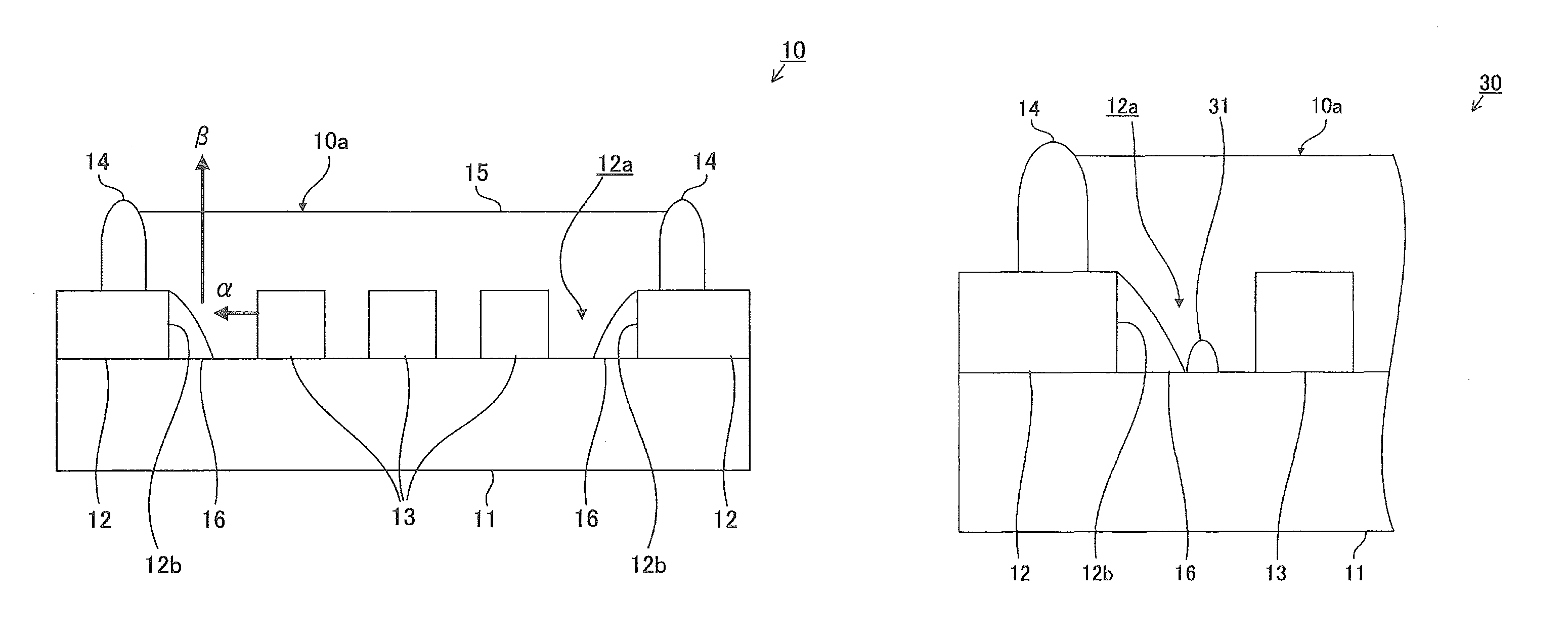
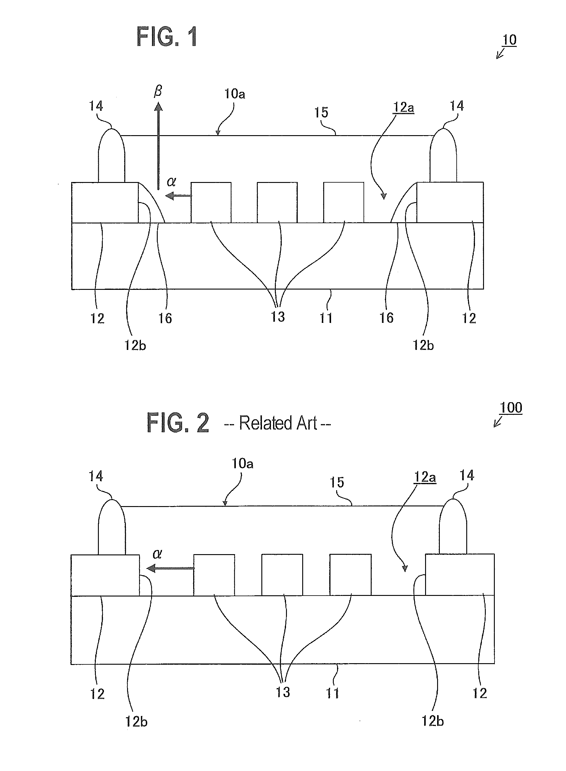
[0055]According to the light emitting device 10 of the first embodiment, the following operation / effect can be obtained.

[0056][1] As shown in FIG. 2, in the light emitting device 100 of the related art, the light reflecting member 16 is not provided and therefore the inner peripheral wall surface 12b of the through-hole 12a of the wiring board 12 is exposed.

[0057]Therefore, as shown by an arrow α in FIG. 2, the light emitted from the side surface of each LED chip 13 is absorbed by the inner peripheral wall surface 12b of the through-hole 12a of the wiring board 12. As a result, there is a problem that the light extraction efficiency is degraded.

[0058]In contrast, in the light emitting device 10, the light emitted from the side surface of each LED chip 13 is irradiated on the light reflecting member 16 which covers the whole inner peripheral wall surface 12b of the through-hole 12a of the wiring board 12, as shown by an arrow α in FIG. 1. Then,...

second embodiment

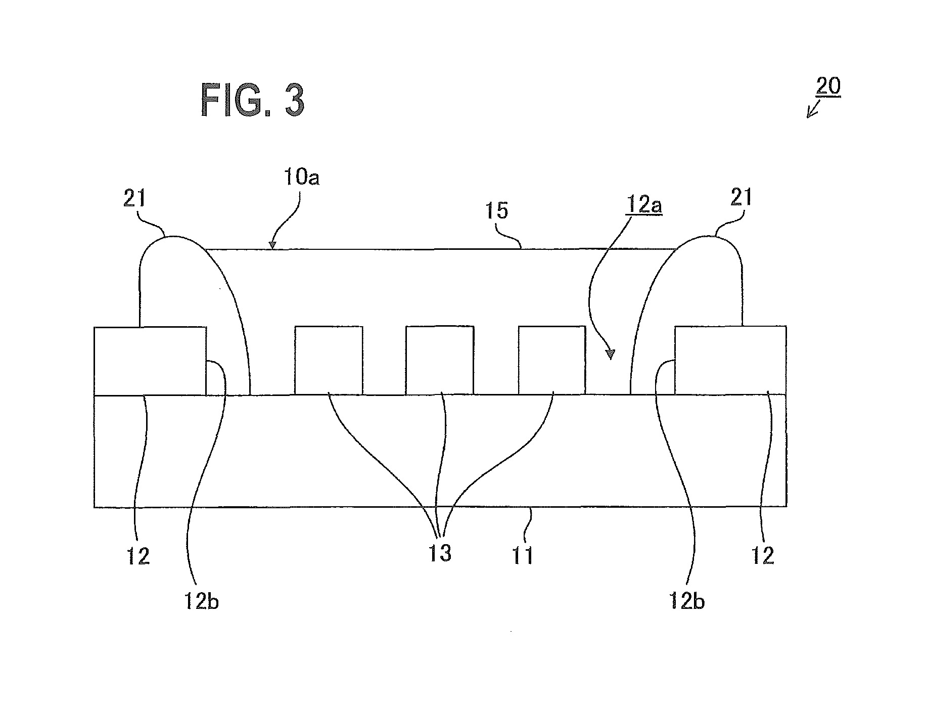
[0065]As shown in FIG. 3, the light emitting device 20 of the second embodiment includes the heat dissipation board 11, the wiring board 12 (the through-hole 12a and the inner peripheral wall surface 12b), the LED chips 13, the frame 14, the encapsulant 15, the light radiating surface 10a and a light reflecting member 21.

[0066]The light emitting device 20 of the second embodiment is different from the light emitting device 10 of the first embodiment only in the fact that the light emitting device 20 includes the light reflecting member 21 which is made by integrating the frame 14 and the light reflecting member 16 of the light emitting device 10.

[0067]In addition to being formed on the surface of the heat dissipation board 11 so as to cover the whole inner peripheral wall surface 12b of the through-hole 12a of the wiring board 12, the light reflecting member 21 is formed on the surface of the wiring board 12 so as to surround the through-hole 12a of the wiring board 12.

[0068]Further...

third embodiment

[0073]As shown in FIG. 4A, the light emitting device 30 of the third embodiment includes the heat dissipation board 11, the wiring board 12 (the through-hole 12a and the inner peripheral wall surface 12b), the LED chips 13, the frame 14, the encapsulant 15, the light reflecting member 16, the light radiating surface 10a and a protrusion member 31.

[0074]The light emitting device 30 of the third embodiment is different from the light emitting device 10 of the first embodiment only in the fact that the light emitting device 30 is provided with the protrusion member 31.

[0075]Therefore, according to the third embodiment, it is possible to obtain the same operation / effect as the first embodiment.

[0076]Further, on the surface of the heat dissipation board 11 that is exposed through the through-hole 12a of the wiring board 12, the protrusion member 31 is formed at a site which is opposed to the inner peripheral wall surface 12b of the through-hole 12a of the wiring board 12 and adjacent to ...


PUM


Abstract

A light emitting device includes a heat dissipation board, a wiring board that is bonded and fixed to the heat dissipation board and formed with a through-hole, a semiconductor light emitting element that is mounted on a face of the heat dissipation board, the face being exposed through the through-hole of the wiring board, and a light reflecting member that covers a portion of an inner peripheral wall surface of the through-hole of the wiring board, the portion being squarely opposed to a side surface of the semiconductor light emitting element.

Description

CROSS-REFERENCE TO RELATED APPLICATIONS[0001]This application claims the benefit of Japanese Patent Application No. 2013-162469 (filed on Aug. 5, 2013), the entire contents of which are hereby incorporated by reference.BACKGROUND[0002]1. Technical Field[0003]The present invention relates to a light emitting device and, more particularly, to a light emitting device including a semiconductor light emitting element.[0004]2. Related Art[0005]JP-A-2007-109701 discloses a board for mounting a light emitting element, having a structure in which a wiring plate and a supporting member are bonded to each other. Here, the wiring plate is provided with a through-hole for passing the reflected light from the supporting member mounted with the light emitting element and the light emitting element is mounted on the supporting member at a position immediately below the through-hole.[0006]JP-A-2011-009298 discloses a light-emitting diode light source which includes a base with thermal conductivity, ...

Claims


Application Information

Patent Timeline
Patent Type & Authority Patents(United States)
IPC IPC(8): H01L33/16H01L33/60H05K1/02H05K3/28H01L25/075H01L33/64
CPCH01L33/60H05K3/284H05K2201/10106H01L2924/0002H01L2924/00H01L25/0753H01L33/644H05K1/021H05K1/0209
Inventor TSUCHIYA, YOSUKETAJIMA, HIROYUKISHIMONISHI, SHOTATAKEDA, SHIGEOMIWA, TOMOHIRO
Owner TOYODA GOSEI CO LTD
Why Eureka
Try Eureka