

Wafer producing method
a production method and technology of wafers, applied in the direction of manufacturing tools, polycrystalline material growth, crystal growth process, etc., can solve the problems of insufficient productivity improvement and application with a very small pitch, and achieve the effect of improving productivity and easy separation
- Summary
- Abstract
- Description
- Claims
- Application Information
AI Technical Summary
Benefits of technology
Problems solved by technology
Method used
Image

Examples
Embodiment Construction
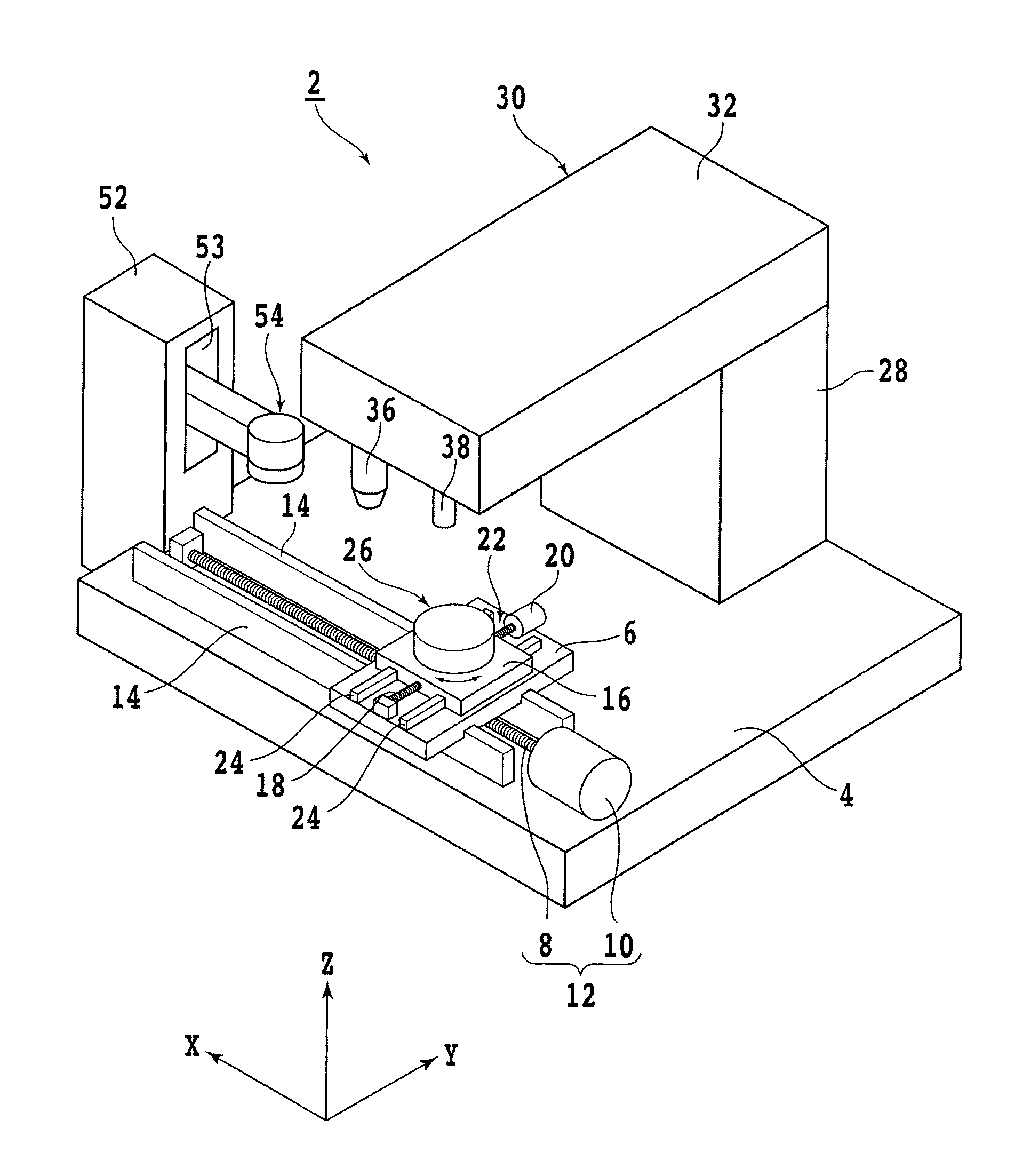
[0028]A preferred embodiment of the present invention will now be described in detail with reference to the drawings. Referring to FIG. 1, there is shown a perspective view of a laser processing apparatus 2 suitable for use in performing a wafer producing method of the present invention. The laser processing apparatus 2 includes a stationary base 4 and a first slide block 6 mounted on the stationary base 4 so as to be movable in the X direction. The first slide block 6 is moved in a feeding direction, or in the X direction along a pair of guide rails 14 by a feeding mechanism 12 composed of a ball screw 8 and a pulse motor 10.
[0029]A second slide block 16 is mounted on the first slide block 6 so as to be movable in the Y direction. The second slide block 16 is moved in an indexing direction, or in the Y direction along a pair of guide rails 24 by an indexing mechanism 22 composed of a ball screw 18 and a pulse motor 20. A support table 26 is mounted on the second slide block 16. The...
PUM
| Property | Measurement | Unit |
|---|---|---|
| diameter | aaaaa | aaaaa |
| off angle | aaaaa | aaaaa |
| off angle | aaaaa | aaaaa |
Abstract
Description
Claims
Application Information