Semiconductor apparatus

a technology of semiconductor and conducting film, which is applied in the direction of semiconductor devices, electrical equipment, basic electric elements, etc., can solve the problems of less processing accuracy of the thick second peripheral conducting film and inability to shorten the clearance between the second peripheral conducting film, etc., and achieve the effect of high electric field

Active Publication Date: 2016-12-27
DENSO CORP
View PDF7 Cites 6 Cited by
  • Summary
  • Abstract
  • Description
  • Claims
  • Application Information

AI Technical Summary

Benefits of technology

[0008]In this semiconductor apparatus, a center of at least one second contact hole is positioned on the inner side than the center line of the corresponding guard ring in the width direction. Accordingly, this second contact hole primarily influences an electric field in the drift region adjacent to the guard ring on the inner side but hardly influences an electric field in the drift region adjacent to the guard ring on the outer side. The electric field generated in the drift region adjacent to the guard ring on the inner side becomes lower than the electric field generated in the drift region adjacent to the guard ring on the outer side. Since the electric field generated in the drift region adjacent to the guard ring on the inner side is low, an electric field that is so high would not be generated even if this region is influenced by the second contact hole. Further, since the influence of the second contact hole hardly affects the drift region adjacent to the guard ring on the outer side, an electric field that is so high would not be generated in this region as well. Accordingly, in this semiconductor apparatus, the generation of the high electric field by the influence of the second contact hole is suppressed.

Problems solved by technology

On the other hand, the thick second peripheral conducting films have less processing accuracy, so a clearance between the second peripheral conducting films cannot be made short.

Method used


Image

  • Semiconductor apparatus
  • Semiconductor apparatus
  • Semiconductor apparatus

Examples


Embodiment Construction

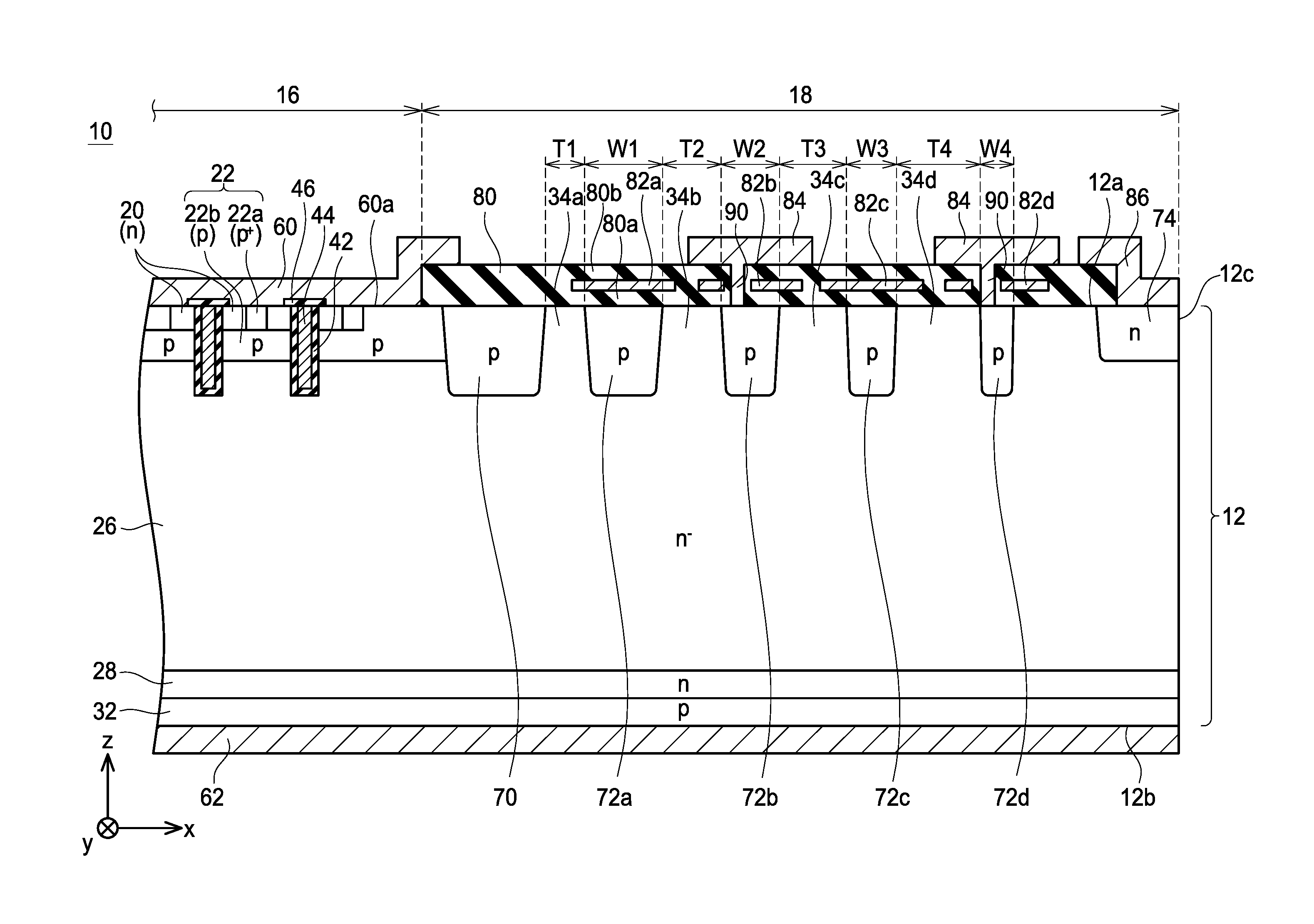
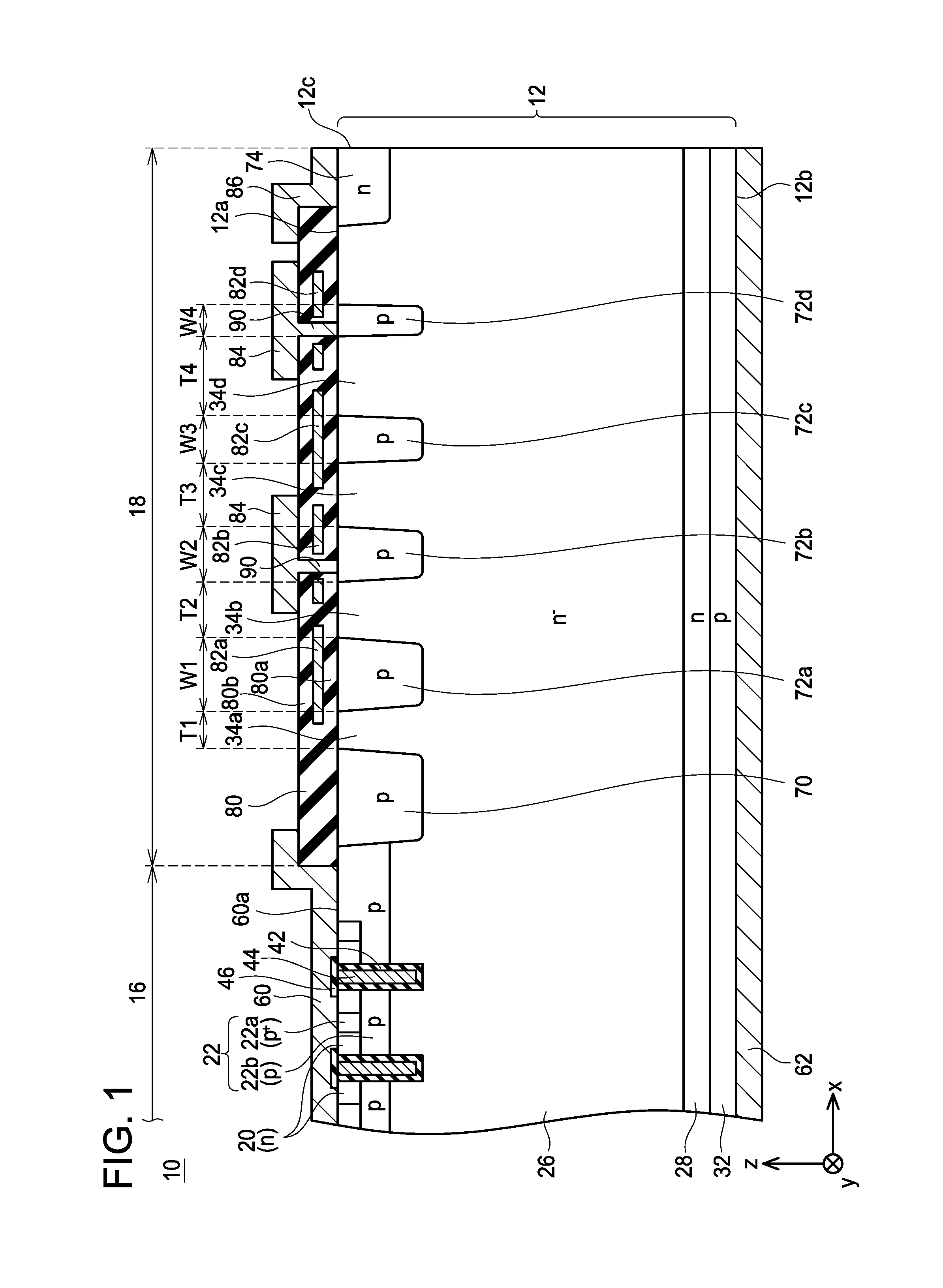
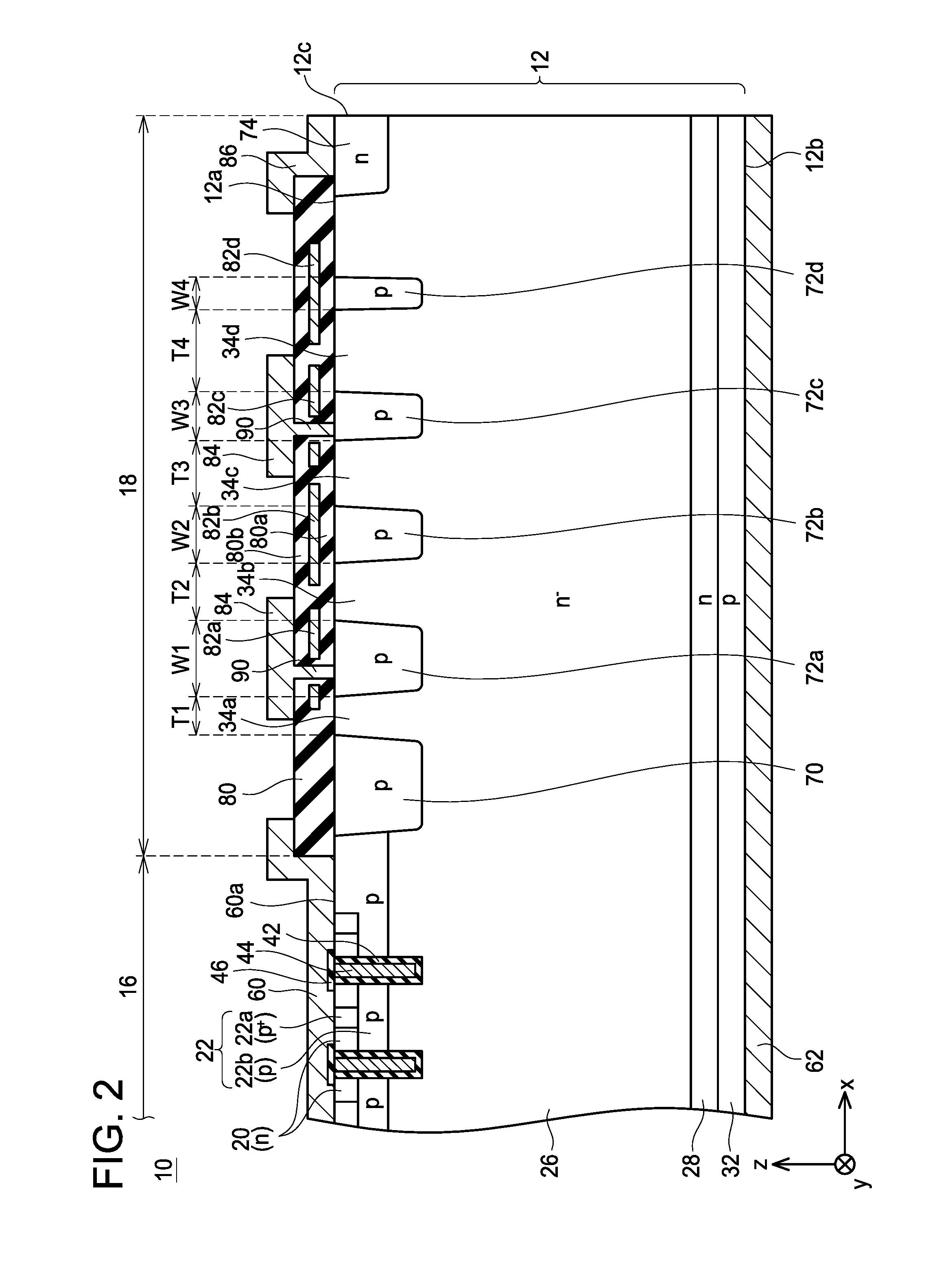
[0023]A semiconductor apparatus 10 shown in FIGS. 1, 2 includes a semiconductor substrate 12 configured by silicon. Notably, hereinbelow, one direction parallel to a front surface 12a of the semiconductor substrate 12 (left and right direction of FIG. 1) will be termed an x direction. Further, a direction that is parallel to the front surface 12a of the semiconductor substrate 12 and orthogonal to the x direction (direction vertical to a sheet surface of FIG. 1) will be termed a y direction. Further, a thickness direction of the semiconductor substrate 12 (up and down direction of FIG. 1) will be termed a z direction.

[0024]A front electrode 60 is provided on the front surface 12a of the semiconductor substrate 12. The front electrode 60 makes contact with the front surface 12a. The front electrode 60 is provided substantially at a center of the front surface 12a of the semiconductor substrate 12. Thus, as shown in FIGS. 3, 4, a contact surface 60a between the semiconductor substrate...


PUM


Abstract

A semiconductor apparatus includes a semiconductor substrate including a device region and a peripheral region. The peripheral region includes guard rings. A first peripheral insulating film, first peripheral conducting films, a second peripheral insulating film and second peripheral conducting films are laminated in the peripheral region. Each of the first peripheral conducting films extends annularly. Each of the second peripheral conducting films overlaps a part of the corresponding first peripheral conducting film. Each of the second peripheral conducting films is connected to the corresponding first peripheral conducting film via a first contact hole. Each of the second peripheral conducting films is connected to the corresponding guard ring via a second contact hole. A center of at least one of the second contact holes is located on inner side with respect to a center line of the guard ring in a width direction.

Description

CROSS-REFERENCE TO RELATED APPLICATION[0001]This application claims priority to Japanese Patent Application No. 2015-107641 filed on May 27, 2015, the contents of which are hereby incorporated by reference into the present application.TECHNICAL FIELD[0002]The technique disclosed herein relates to a semiconductor apparatus.BACKGROUND ART[0003]WO 2013 / 140572 A1 discloses a semiconductor apparatus provided with a plurality of guard rings surrounding a device region where an IGBT (Insulated Gate Bipolar Transistor) is formed. Each guard ring is configured of a p-type region provided in an n-type semiconductor substrate, and is provided at a position exposed in a front surface of the semiconductor substrate. Each guard ring extends in an annular shape surrounding the device region, and the plurality of guard rings surrounds the device region in multiple layers. Further, the semiconductor apparatus includes first peripheral conducting films and second peripheral conducting films. The firs...

Claims


Application Information

Patent Timeline
Patent Type & Authority Patents(United States)
IPC IPC(8): H01L29/06H01L29/40
CPCH01L29/0623H01L29/0696H01L29/404H01L29/0619H01L29/7395H01L29/7827H01L29/7397H01L29/7813H01L29/8611H01L29/0638H01L29/1095H01L29/7811
Inventor SENOO, MASARU
Owner DENSO CORP
Why Eureka
Try Eureka