Substrate for organic electronic device

a technology of organic electronic devices and substrates, which is applied in the direction of solid-state devices, sustainable manufacturing/processing, and final product manufacturing, etc., can solve the problems of difficult control of sheet resistance, uneven emission of light, so as to achieve excellent luminance and emission uniformity, and efficiently control the sheet resistance of the electrode

Active Publication Date: 2017-01-03
LG DISPLAY CO LTD
View PDF35 Cites 6 Cited by
  • Summary
  • Abstract
  • Description
  • Claims
  • Application Information

AI Technical Summary

Benefits of technology

[0009]When an OLED is formed above an exemplary substrate of the present invention, even when the OLED is formed in a large size, the substrate can ensure excellent luminance and emission uniformity by efficiently controlling a sheet resistance of an electrode.

Problems solved by technology

Since the OLED has a large emitting area as described above, if a sheet resistance of an electrode is high, electrons or holes are not uniformly injected throughout an entire area, thereby generating an emitting spot, or uniform luminance may not be obtained from an entire emitting region.
Particularly, the transparent electrode may not have an excessively high thickness to ensure transparency, and thus it is not easy to control the sheet resistance.

Method used


Image

  • Substrate for organic electronic device
  • Substrate for organic electronic device
  • Substrate for organic electronic device

Examples


example 1

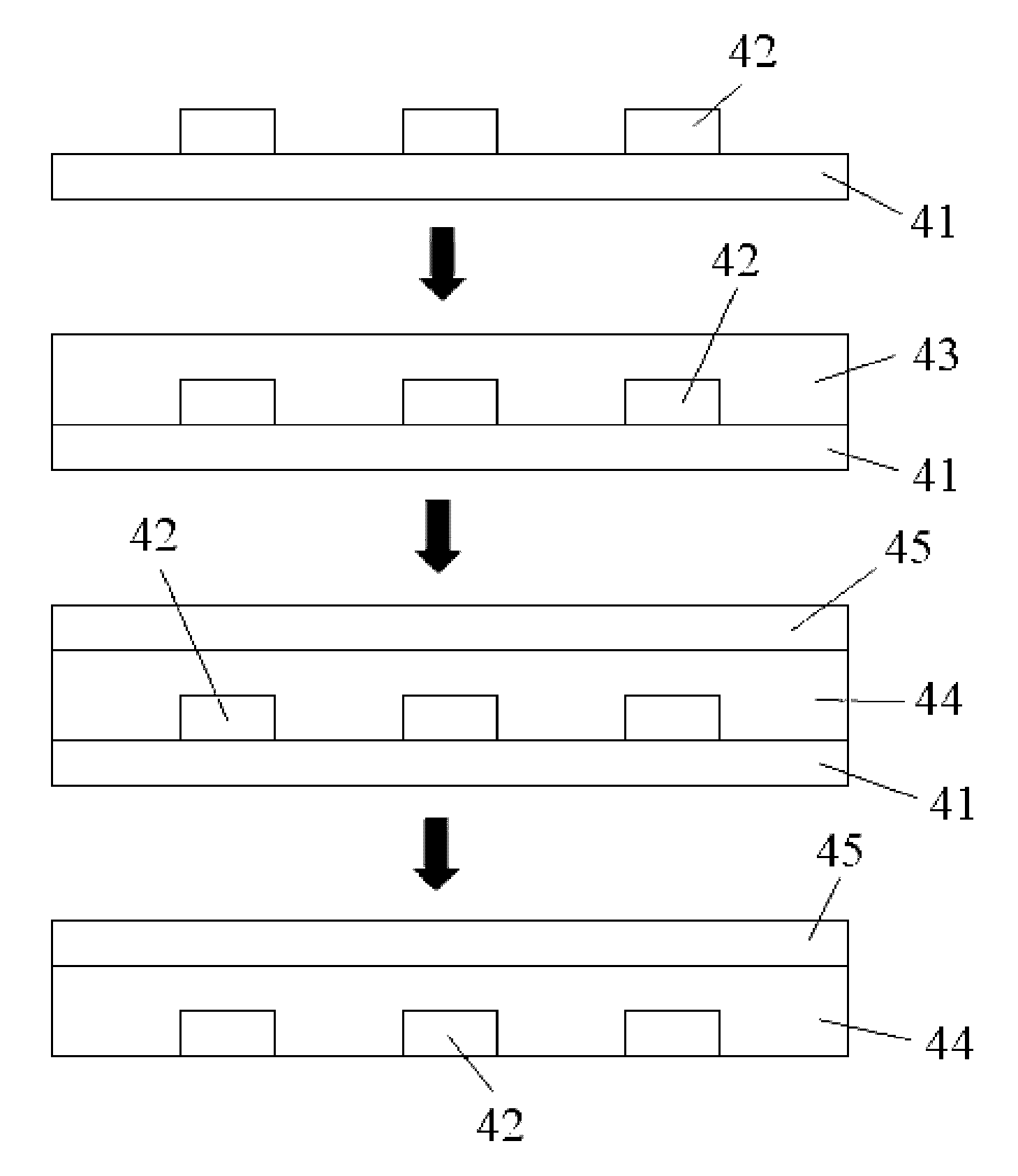
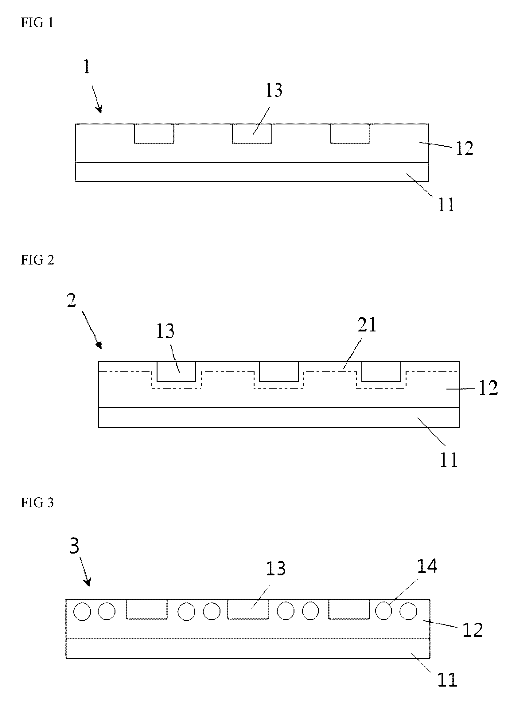
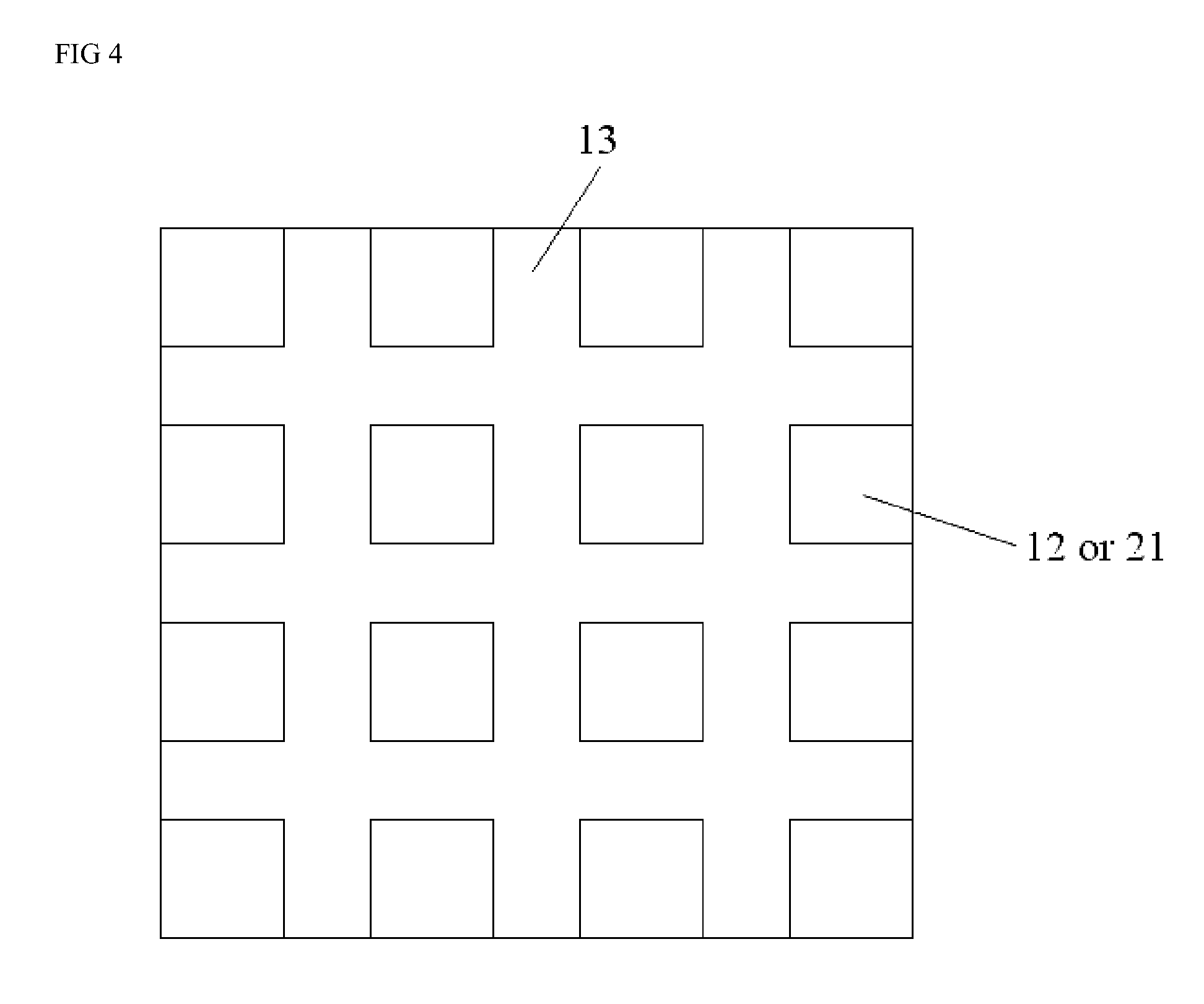
[0077]A grid-shaped conductive pattern was printed on a surface of a PET film which was not treated with a primer by an offset gravure printing method using an Ag paste. In this operation, a line width of the conductive pattern was controlled to 20 μm, and a gap between lines thereof was controlled to 280 μm, and a height thereof was controlled to approximately 1 μm. Afterward, the printed conductive pattern was plasticized at a temperature of 150° C. for about 30 minutes. Subsequently, a UV curable adhesive composition (NOA65, Norland Products Inc.) was coated on a surface of the PET film on which the conductive pattern was formed, and a glass substrate was laminated thereon and compressed with a rubber roller to sufficiently spread the composition. Afterward, an adhesive layer was formed by radiating a UV ray (2 J / cm2) onto the composition. After the formation of the adhesive layer, the PET film was peeled off, thereby obtaining a substrate for an OED. FIGS. 7 and 8 show images of...

example 2

[0078]A substrate was manufactured by the same method as described in Example 1, except that, in the formation of a conductive pattern, a line width 40 μm, a gap between lines 260 μm, and a height about 2 μm were controlled.

example 3

[0079]A grid-shaped conductive pattern was printed on a surface of a PET film which was not treated with a primer by an offset gravure printing method using an Ag paste. In this operation, a line width of the conductive pattern was controlled to 20 μm, a gap between lines thereof was controlled to 280 μm, and a height thereof was controlled to approximately 1 μm. Afterward, the printed conductive pattern was plasticized at a temperature of 150° C. for about 30 minutes. Subsequently, a coating solution (TYT-80-01, Toyo ink) for forming a surface layer was coated on a surface of the PET film on which the conductive pattern was formed, dried at 100° C. for about 10 minutes, and cured by radiating a UV ray, thereby forming a surface layer. Subsequently, a UV curable adhesive composition (NOA65, Norland Products Inc.) was coated on a substrate on which the conductive pattern and the surface layer were formed, and a glass substrate was laminated thereon and compressed with a rubber roller...


PUM


Abstract

The present invention relates to a substrate for an organic electrode device, a manufacturing method thereof, and an organic electronic device. An exemplary substrate of the invention, if an organic light emitting element is formed on an upper part of the substrate, can obtain luminance with high emission and uniformity by efficiently controlling the surface resistance of an electrode even when the device is configured into larger sizes.

Description

[0001]This application is a Continuation of U.S. application Ser. No. 14 / 036,858, filed Sep. 25, 2013, and which is a Continuation Bypass of International Application No. PCT / KR2012 / 002338, filed Mar. 29, 2012, which claims priority to and the benefit of Korean Patent Application Nos. 10-2011-0028091, filed on Mar. 29, 2011, and 10-2011-0102473, filed on Oct. 7, 2011, the disclosures of which are incorporated herein by reference in their entirety.TECHNICAL FIELD[0002]The present invention relates to a substrate for an organic electronic device, a method of manufacturing the substrate, and an organic electronic device.BACKGROUND ART[0003]An organic electronic device (OED) may be a device exhibiting various functions through exchange of charges between an electrode and an organic material, and for example of the OED may be included an organic light emitting device (OLED), an organic solar cell, an organic photo conductor (OPC) or an organic transistor and the like.[0004]In the OED, el...

Claims


Application Information

Patent Timeline
Patent Type & Authority Patents(United States)
IPC IPC(8): H01L51/00H01L51/52H01L51/42H01L51/50
CPCH01L51/0023H01L51/003H01L51/0096H01L51/5268H01L51/42H01L51/50H01L51/5212H01L51/5228H01L51/5262Y02E10/549Y02P70/521H10K71/621H10K71/80H10K77/10H10K30/00H10K50/00H10K50/854Y02P70/50H10K30/83H10K50/814H10K50/824H10K50/85
Inventor LEE, YEON KEUNMOON, KYOUNG SIKJANG, SEONG SOOAHN, YONG SIKKIM, JUNG DOOPARK, MIN CHOONKIM, JUNG BUM
Owner LG DISPLAY CO LTD
Why Eureka
Try Eureka