Low-noise arrangement for very-large-scale integration differential input/output structures

a technology of differential input/output structure and low-noise arrangement, which is applied in the direction of electrical apparatus, semiconductor devices, semiconductor/solid-state device details, etc., can solve the problems of increasing the complexity of interfacing with those ics, and the integration circuit is becoming increasingly complex, so as to reduce noise, suppress noise, and eliminate noise

Active Publication Date: 2017-01-10
ORACLE INT CORP
View PDF3 Cites 4 Cited by
  • Summary
  • Abstract
  • Description
  • Claims
  • Application Information

AI Technical Summary

Benefits of technology

[0004]Among other things, systems and methods are described for providing low-noise arrangements for VLSI differential input / output (I / O) structures. The I / O structures can include I / O pins, solder bumps, ball grid array (BGA) solder balls, vias, and / or other physical (e.g., vertical) structures of an integrated circuit (IC) that carry differential signals or supply levels to and / or from circuits of the IC. Novel perpendicular quad (PNQ) and triangular quad (TNQ) geometries are described for arranging differential pairs of I / O structures in perpendicular or near-perpendicular “quads.” The geometries effectively place one differential pair on or near the perpendicular bisector of its adjacent differential pair, such that field cancellation and differential reception can substantially eliminate noise without the need for added spacing or shields. By exploiting these effects, embodiments can suppress noise, independent of I / O structure spacing, and arbitrarily small spacings are permitted. Such arrangements can be extended into running chains, and even further into arrays of parallel chains. The parallel chains can be separated by supply structures (e.g., power supply bumps, or the like), and such supply structures can supply power to the I / O circuits of the IC, while also shielding adjacent chains from each other.

Problems solved by technology

Integrated circuits are becoming increasingly complex.
Such increases tend to increase the complexity of interfacing with those ICs.
Often, there is also a desire to operate ICs with high signal integrity, which can be difficult with large numbers of densely arranged I / O structures.

Method used


Image

  • Low-noise arrangement for very-large-scale integration differential input/output structures
  • Low-noise arrangement for very-large-scale integration differential input/output structures
  • Low-noise arrangement for very-large-scale integration differential input/output structures

Examples


Embodiment Construction

[0017]In the following description, numerous specific details are set forth to provide a thorough understanding of the present invention. However, one having ordinary skill in the art should recognize that the invention may be practiced without these specific details. In some instances, circuits, structures, and techniques have not been shown in detail to avoid obscuring the present invention.

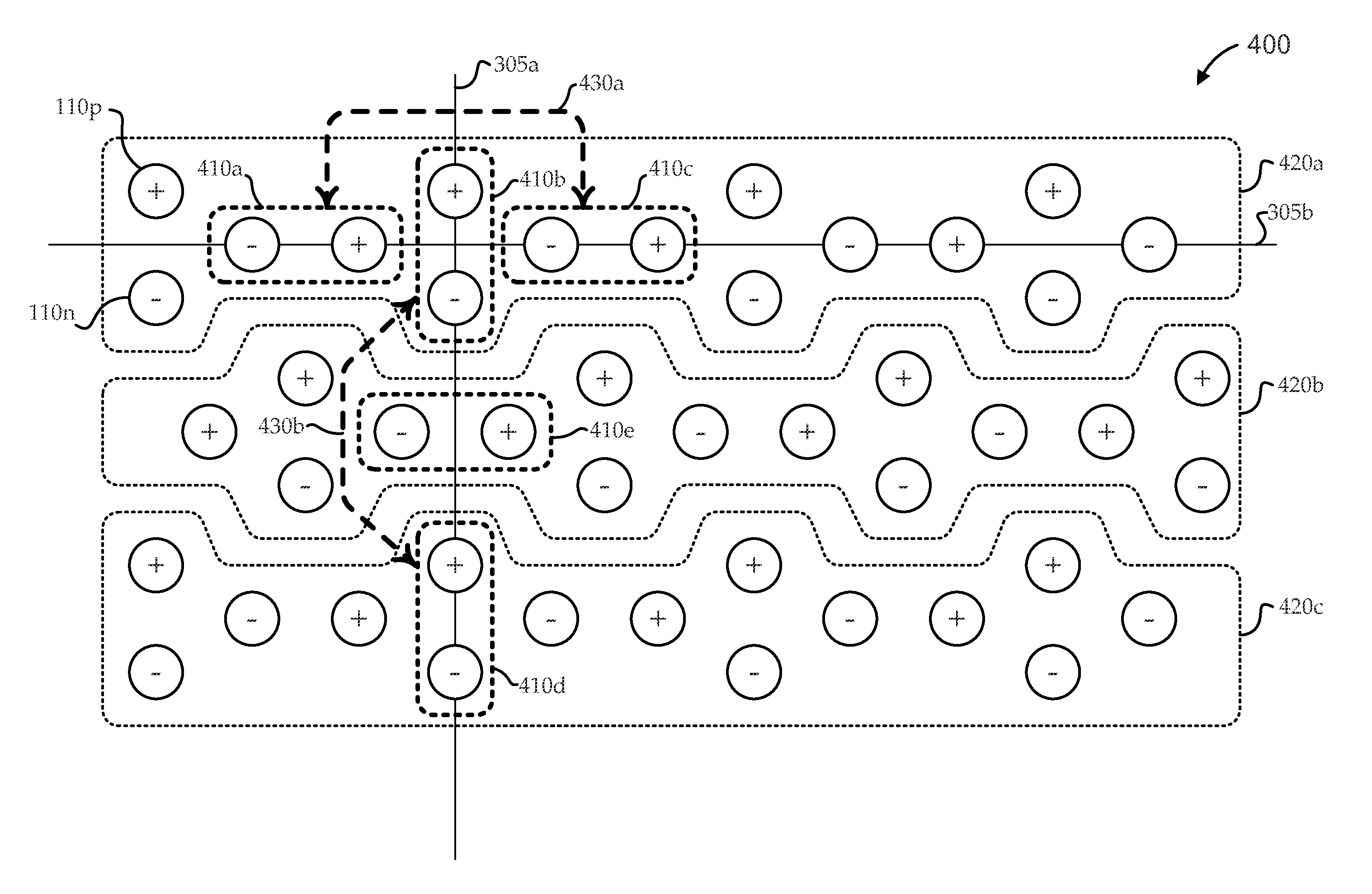
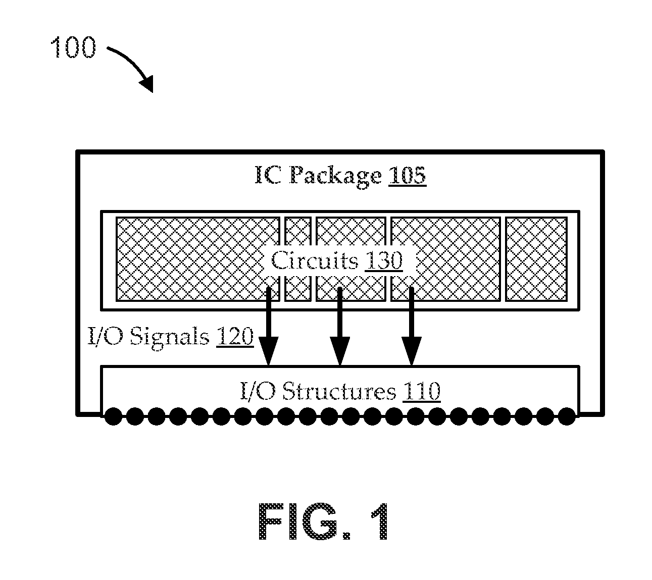
[0018]For the sake of context, FIG. 1 shows an illustrative simplified view of a very-large-scale integration (VLSI) integrated circuit (IC) 100. The IC 100 includes a number of circuits 130. Various ones of the circuits 130 can transmit and / or receive various types of signals, including I / O signals 120. The I / O signals 120 can be communicated between the circuits 130 of the IC 100 and systems external to the IC 100 (e.g., other circuits, etc.) via I / O structures 110. As used herein, the term “I / O structure” is intended to broadly refer to any suitable interface structure for an IC, including, ...


PUM


Abstract

Embodiments of the invention provide low-noise arrangements for very-large-scale integration (VLSI) differential input / output (I / O) structures (I / O pins, solder bumps, vias, etc.). Novel geometries are described for arranging differential pairs of I / O structures in perpendicular or near-perpendicular “quads.” The geometries effectively place one differential pair on or near the perpendicular bisector of its adjacent differential pair, such that field cancellation and differential reception can substantially eliminate noise without the need for added spacing or shields. By exploiting these effects, embodiments can suppress noise, independent of I / O structure spacing, and arbitrarily small spacings are permitted. Such arrangements can be extended into running chains, and even further into arrays of parallel chains. The parallel chains can be separated by supply structures (e.g., power supply bumps, or the like), and such supply structures can supply power to the I / O circuits of the IC, while also shielding adjacent chains from each other.

Description

BACKGROUND[0001]Embodiments relate generally to very-large-scale integration (VLSI) integrated circuits, and, more particularly, to low-noise arrangements for VLSI differential input / output (I / O) structures.[0002]Integrated circuits are becoming increasingly complex. For example, in VLSI integrated circuit (IC) design, there has been a trend towards increasing die sizes, numbers of circuits, compaction of circuits, etc. Such increases tend to increase the complexity of interfacing with those ICs. For example, interfacing with higher numbers and densities of signals being communicated to and from the circuits of the IC can involve higher numbers and densities of pins, solder bumps, and / or other vertical I / O structures.[0003]Often, there is also a desire to operate ICs with high signal integrity, which can be difficult with large numbers of densely arranged I / O structures. For example, many I / O signals can be communicated as differential signals (e.g., by pairs of pins), which can per...

Claims


Application Information

Patent Timeline
Patent Type & Authority Patents(United States)
IPC IPC(8): H01L23/52H01L23/00H01L23/522
CPCH01L23/5226H01L24/17H01L24/49H01L23/5286H01L2924/00014H01L2224/45099H01L2224/45015H01L2924/207
Inventor MASLEID, ROBERT P.DRAPER, DONALD ARTHURKUNZ, EBENKOCUBINSKI, LAURA
Owner ORACLE INT CORP
Why Eureka
Try Eureka