Package substrate and flip-chip package circuit including the same

a technology of packaging substrate and flip-chip package circuit, which is applied in the direction of printed circuit non-printed electric components, semiconductor devices, semiconductor/solid-state device details, etc., can solve the problems of poor yield rate and reliability of products, insufficient affinity between primer materials and metal pillars or molding compounds, and high cost and restriction of primer materials

Active Publication Date: 2017-01-17
PHOENIX PIONEER TECH
View PDF3 Cites 0 Cited by
  • Summary
  • Abstract
  • Description
  • Claims
  • Application Information

AI Technical Summary

Benefits of technology

[0003]A next-generation electronic product is asked to have multiple functions and high-speed performance other than compactness. The integrated-circuit manufacturers have moved to smaller design rules to make chips with much more electronic devices. On the other hand, the techniques for packaging the chips or semiconductor substrates have also been developed for the same purpose.
[0023]In the existing FCCSP fabrication, a photo-sensitive primer material is used in the formation of the dielectric material layer on the molding compound layer, so it is highly required to have an enough resolution of photolithography in the fabrication process. Especially for the package manufacturing process of fine pitch, the primer material is expensive and restricted to some specific chemical compositions. As shown in FIG. 1, each of the metal pillars may include an upper segment 19 in the dielectric material layer 17 and a lower segment 18 in the conductive pillar layer 16, which are respectively formed in different photolithography processes of the molding compound layer 16 and the dielectric material layer 17. There may be location deviations between the two segments 18 and 19 caused by the possible photo-mask misalignments among the photolithography processes. Also, the affinity between the primer material and either the metal pillar or the molding compound may not strong enough. These may make yield rate and reliability of the product worse. To avoid the above-described problems, we design a package substrate 100 as shown in FIG. 2 in the present disclosure. The molding compound layer 136 can be divided into two areas, a first area A and a second area B, as shown in FIG. 4E. The part of the molding compound layer 136 in the second area B is higher than that in the first area A, and the difference therebetween is the protrusion part 135 which surrounds the upper part of the metal pillars 131-133. That is to say, side surfaces of the metal pillars 131-133 are completely covered by the molding compound layer 136 in the second area B. In the embodiments, the protrusion part 135 may have an increasing width from top to bottom, with its upper-part narrower than its lower-part. Preferably, the protrusion part 135 may have a hyperbolic or parabolic concave side wall. Thus, the metal pillars 131-133 can be formed in only one single photolithography step by adopting proper composition material for both of the molding compound layer 136 and the second dielectric material layer 138 as well as setting up a proper fabrication process for the conductive pillar layer 130.

Problems solved by technology

Especially for the package manufacturing process of fine pitch, the primer material is expensive and restricted to some specific chemical compositions.
Also, the affinity between the primer material and either the metal pillar or the molding compound may not strong enough.
These may make yield rate and reliability of the product worse.

Method used


Image

  • Package substrate and flip-chip package circuit including the same
  • Package substrate and flip-chip package circuit including the same
  • Package substrate and flip-chip package circuit including the same

Examples


Embodiment Construction

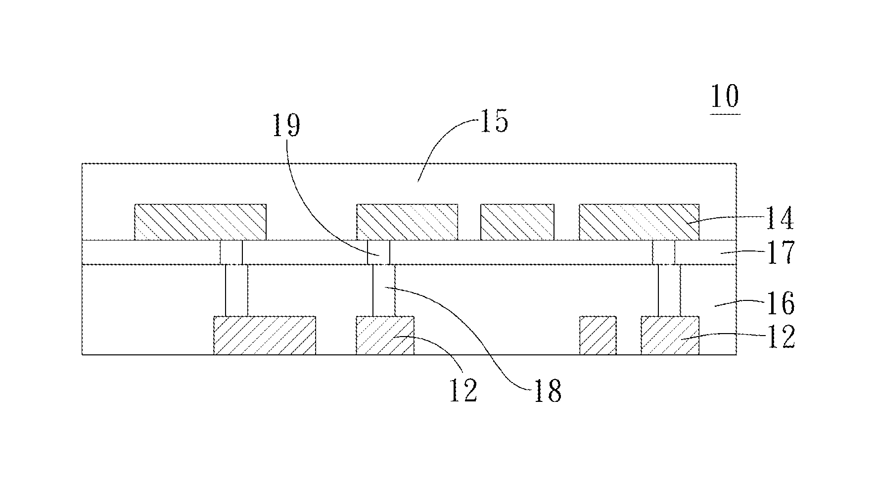
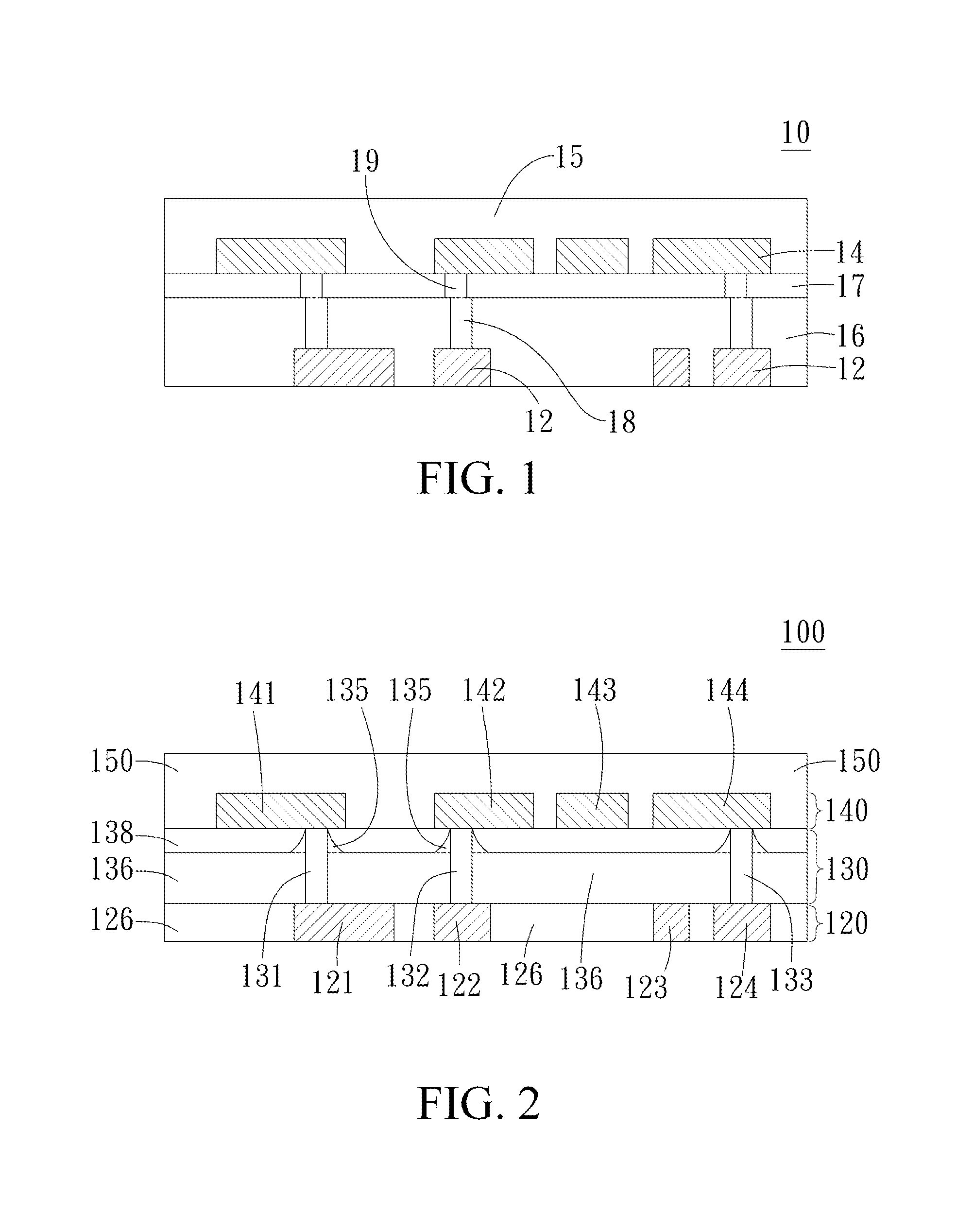
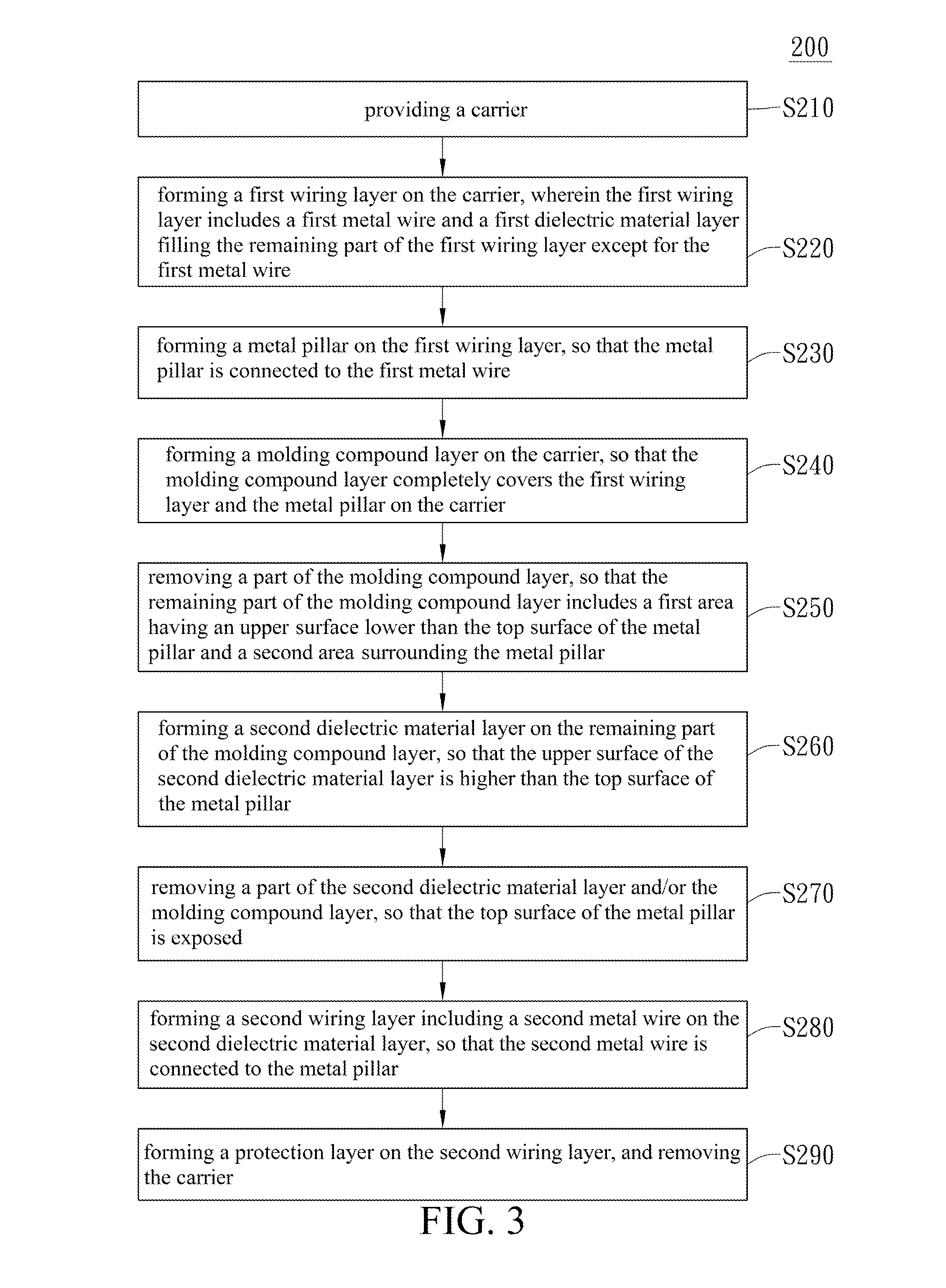
[0018]For further understanding and recognizing the fulfilled functions and structural characteristics of the disclosure, several exemplary embodiments cooperating with detailed description are presented as the following. Reference will now be made in detail to the preferred embodiments, examples of which are illustrated in the accompanying drawings.

[0019]In the following description of the embodiments, it is to be understood that when an element such as a layer (film), region, pattern, or structure is stated as being “on” or “under” another element, it can be “directly” on or under another element or can be “indirectly” formed such that an intervening element is also present. Also, the terms such as “on” or “under” should be understood on the basis of the drawings, and they may be used herein to represent the relationship of one element to another element as illustrated in the figures. It will be understood that this expression is intended to encompass different orientations of the...


PUM


Abstract

This disclosure provides a package substrate, a flip-chip package circuit and their fabrication method. The package substrate includes: a first wiring layer having a first metal wire and a first dielectric material layer filling the remaining part of the first wiring layer except for the first metal wire; a conductive pillar layer formed on the first wiring layer and including a metal pillar connected to the first metal wire, a molding compound layer with a protrusion part surrounding the metal pillar, and a second dielectric material layer formed on the molding compound layer; a second wiring layer formed on the conductive pillar layer and including a second metal wire connected to the metal pillar; and a protection layer formed on the second wiring layer.

Description

[0001]This application claims the benefit of Taiwan application Serial No. 103120893, filed on Jun. 17, 2014, and the disclosure of which is incorporated by reference herein in its entirety.TECHNICAL FIELD[0002]The present disclosure relates to a package substrate, a flip-chip package circuit, and their fabrication methods.TECHNICAL BACKGROUND[0003]A next-generation electronic product is asked to have multiple functions and high-speed performance other than compactness. The integrated-circuit manufacturers have moved to smaller design rules to make chips with much more electronic devices. On the other hand, the techniques for packaging the chips or semiconductor substrates have also been developed for the same purpose.[0004]Conventionally, a flip-chip chip size package (FCCSP) substrate 10 used to construct the so-called “molded interconnection substrate (MIS)” can be illustrated in FIG. 1. A photo-sensitive primer material can be used in the formation of the dielectric material lay...

Claims


Application Information

Patent Timeline
Patent Type & Authority Patents(United States)
IPC IPC(8): H05K1/18H01L21/683H01L23/498H01L21/48H01L23/31
CPCH01L21/6835H01L21/486H01L21/4857H01L23/31H01L23/49822H01L23/49827H01L23/49816H01L23/49894H01L2221/68345H01L2924/0002H01L2924/00
Inventor HSU, CHE-WEIHSU, SHIH-PING
Owner PHOENIX PIONEER TECH
Why Eureka
Try Eureka