TFT array substrate and display device with tilt angle between strip-like pixel electrodes and direction of initial alignment of liquid crystals
a technology of thin film transistors and array substrates, applied in non-linear optics, instruments, optics, etc., can solve the problems of not resolving black stripes at the edges of pixels, forgoing existing technologies, etc., to improve reduce regions of orientation disorder of liquid crystals at the edge of pixel units, and improve the effect of aperture ratio and transmittan
- Summary
- Abstract
- Description
- Claims
- Application Information
AI Technical Summary
Benefits of technology
Problems solved by technology
Method used
Image

Examples
embodiment 1
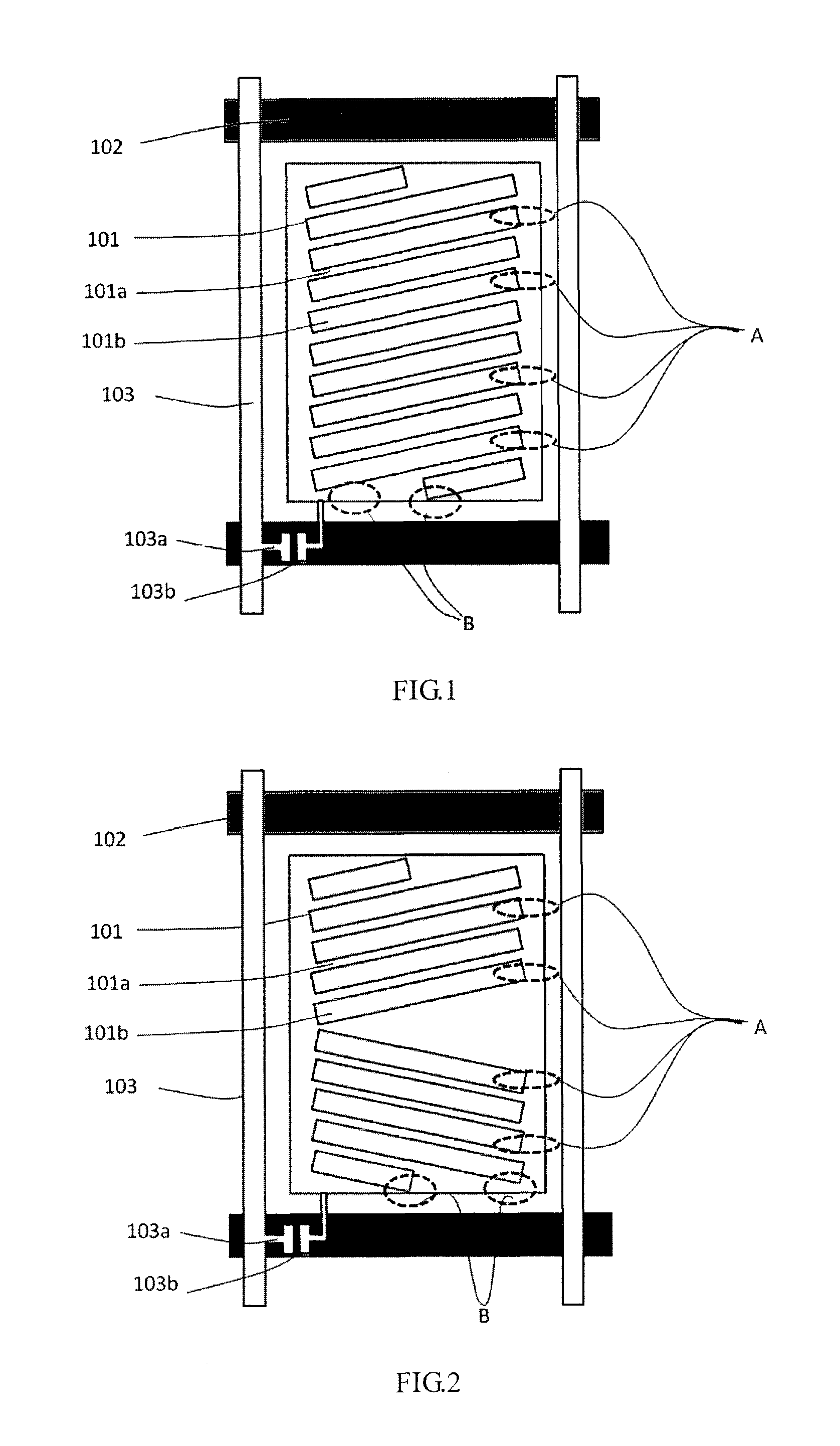
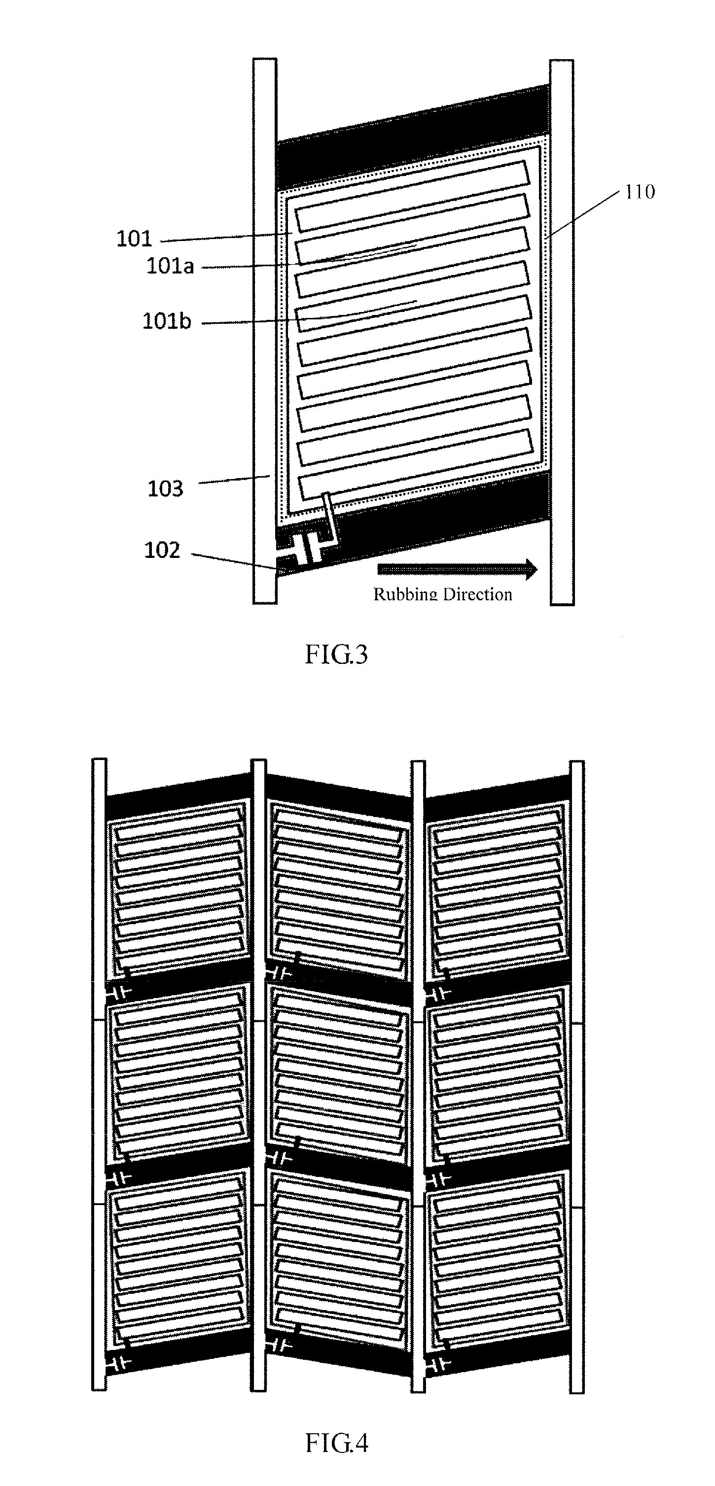
[0033]FIG. 3 is a schematic view illustrating the structure of a single sub-pixel in a TFT array substrate structure according to the invention. The array substrate comprises a plurality of gate lines 102 and a plurality of data lines 103 which are formed on a base substrate (not shown in the figure); and a plurality of sub-pixel units defined by intersecting each other of these gate lines 102 and data lines 103, each of the sub-pixel units comprising a thin film transistor device as a switching element and a common electrode, a first pixel electrode layer 110 and a second pixel electrode layer 101. The first pixel electrode layer 110, as shown by a broken-line in FIG. 3, comprises a plate-like electrode, for example. On the second pixel electrode layer 101, there are strip-like pixel electrodes 101a and openings 101b of the second pixel electrode layer 101. One of the first pixel electrode layer 110 and the second pixel electrode layer 101 is connected to the common electrode, the ...
embodiment 2
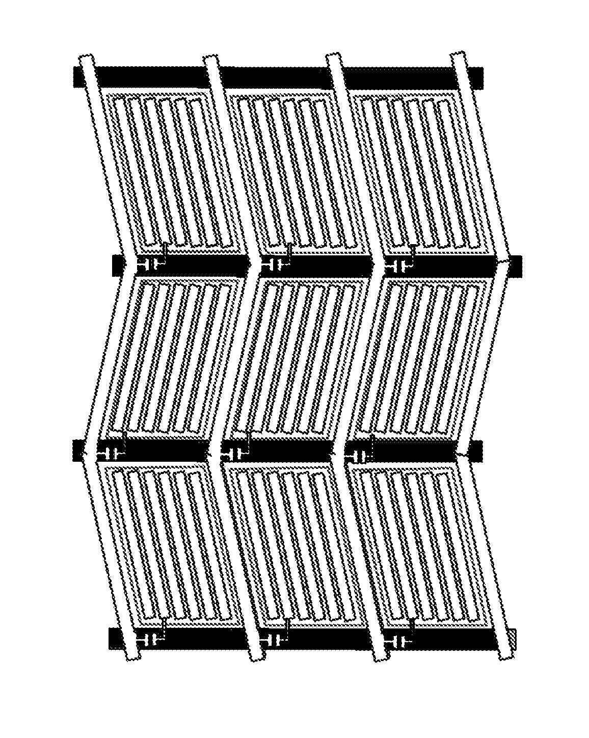
[0037]As shown in FIG. 5, it differs from Embodiment 1 in that: an alignment layer located on an array substrate is, for example, rubbed in a perpendicular direction as shown in FIG. 5, so that the initial orientation of liquid crystals is a vertical direction, data lines 103 are parallel to strip-like pixel electrodes 101a, the direction of gate lines 102 is perpendicular to the initial orientation of the liquid crystals, and entire second pixel electrode layer 101 takes the shape of parallelogram.
[0038]Such a design makes direction of a disturbed electric field produced by the data lines 103 consistent with direction of a fringe field for driving the liquid crystals within the pixel units, and meanwhile, pixel-electrode edges close to the data lines 103 are parallel to the inside strip-like pixel electrodes 101a. This will not cause a phenomenon of orientation disorder of liquid crystals at edges of the pixel units due to influence of disordered electric fields, and will cause no ...
embodiment 3
[0040]As shown in FIG. 7, it differs from Embodiment 1 in that: in each of sub-pixel units, the plurality of strip-like pixel electrodes 101a on the second pixel electrode layer 101 are divided into two sets which are symmetric to each other with respect to the central line of the sub-pixel unit for example, and respective strip-like pixel electrodes 101a in each of the sets are parallel to each other. Each of the two gate lines 102 surrounding the sub-pixel unit is parallel to the corresponding one of the sets of the strip-like pixel electrodes 101a close to the gate lines in the second pixel electrode layer, so that entire second pixel electrode layer 101 of the sub-pixel unit take the shape of trapezoid.
[0041]In the embodiment, an alignment layer located on an array substrate is, for example, rubbed in a horizontal direction as shown in FIG. 7, so that the initial orientation of liquid crystals is horizontal.
[0042]Such a design makes direction of a disturbed electric field produc...
PUM
 Abstract
Description
Claims
Application Information
 - R&D
- Intellectual Property
- Life Sciences
- Materials
- Tech Scout
- Unparalleled Data Quality
- Higher Quality Content
- 60% Fewer Hallucinations
Browse by: Latest US Patents, China's latest patents, Technical Efficacy Thesaurus, Application Domain, Technology Topic, Popular Technical Reports.
© 2025 PatSnap. All rights reserved.Legal|Privacy policy|Modern Slavery Act Transparency Statement|Sitemap|About US| Contact US: help@patsnap.com