Array substrate and display device

a substrate and array technology, applied in the field of array substrates, can solve the problems of reducing the pixel aperture ratio and the inability to drive liquid crystals, and achieve the effect of improving the pixel aperture ratio and thus the quality of the devi

Active Publication Date: 2017-05-30
TRIVALE TECH
View PDF29 Cites 3 Cited by
  • Summary
  • Abstract
  • Description
  • Claims
  • Application Information

AI Technical Summary

Benefits of technology

[0008]The present invention has been made in view of the above-mentioned problems, and an object thereof is to provide the technology capable of improving a pixel aperture ratio, and thus device quality.
[0010]The pixel aperture ratio, and thus device quality can be improved.

Problems solved by technology

In this liquid crystal display device, unfortunately, an alignment film formed on a region near the connection portion cannot be rubbed reliably due to the unevenness of the connection portion (contact hole), resulting in a problem that the liquid crystals may not be driven.
This results in narrower areas for pixels, causing a problem that a pixel aperture ratio decreases.

Method used


Image

  • Array substrate and display device
  • Array substrate and display device
  • Array substrate and display device

Examples


first preferred embodiment

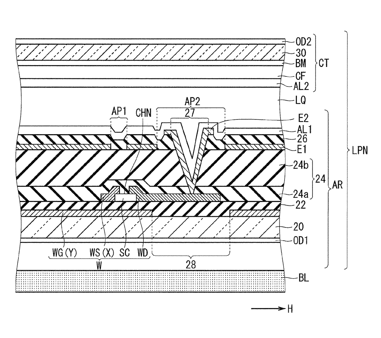
[0016]A case in which the present invention is applied to a liquid crystal display device whose liquid crystal mode is the fringe field switching (FFS) mode is described below as a first preferred embodiment of the present invention. FIG. 1 is a cross-sectional view showing the configuration of the liquid crystal display device according to the first preferred embodiment. FIG. 1 is described schematically and does not correctly reflect, for example, the sizes of elements shown. In addition, the portion other than the main portion of the invention is omitted or partially simplified where appropriate for brevity (the same holds true for the drawings below). Further, in the drawings, like references refer to like or similar elements, and description thereof is omitted.

[0017]

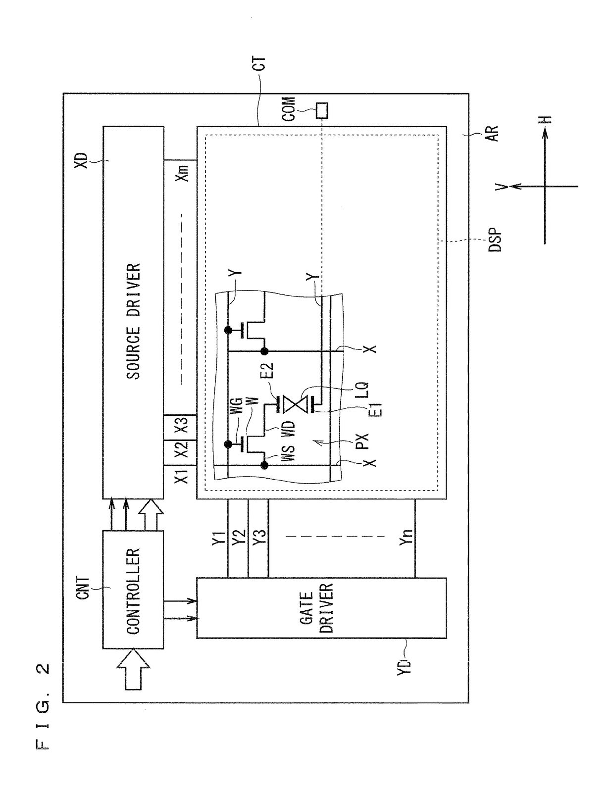
[0018]As shown in FIG. 1, the liquid crystal display device includes a transmissive liquid crystal display panel LPN and an illumination unit, namely backlight unit BL.

[0019]The liquid crystal display panel LPN incl...


PUM

PropertyMeasurementUnit
widthaaaaaaaaaa
insulatingaaaaaaaaaa
electric fieldaaaaaaaaaa

Abstract

An array substrate includes a first electrode located above a switching element through a first insulating film, a second electrode located above the first electrode through a second insulating film, and a connection portion that is located to pass through the first insulating film, first electrode, and second insulating film and electrically connects a drain electrode of the switching element and the second electrode. The connection portion is disposed in an avoidance region provided by carving out a gate line connected to the switching element.

Description

BACKGROUND OF THE INVENTION[0001]Field of the Invention[0002]The present invention relates to an array substrate having a switching element in a display device, and a display device including the same.[0003]Description of the Background Art[0004]The twisted nematic (TN) mode has been widely used as a display type of a liquid crystal display device that is a type of display device. Recently, the transverse electric field type liquid crystal display device has been proposed, in which a voltage is applied between the first and second electrodes provided in one substrate to generate an electric field almost parallel to the panel, whereby the liquid crystal molecules are driven horizontally. The transverse electric field type is advantageous in wider viewing angle, higher resolution and higher brightness and is now becoming mainstream particularly in middle or small sized panels such as smartphones and tablets.[0005]Display types such as in plane switching (IPS) mode and fringe field swi...

Claims


Application Information

Patent Timeline
Patent Type & Authority Patents(United States)
IPC IPC(8): H01L27/12G02F1/13G02F1/1362G02F1/1343
CPCH01L27/124G02F1/136227G02F1/136286G02F2001/134372G02F1/134372
Inventor HOKA, NARUHITOTANAHARA, MANABUSHIMAMURA, TAKESHI
Owner TRIVALE TECH
Why Eureka
Try Eureka