Supercharge Your Innovation With Domain-Expert AI Agents!

Integration of laminate MEMS in BBUL coreless package

a technology of laminate mems and coreless packages, applied in the direction of printed circuit non-printed electric components, instruments, television systems, etc., can solve the problems of limited die size and the available space for placemen

Active Publication Date: 2017-07-18
INTEL CORP
View PDF9 Cites 0 Cited by
  • Summary
  • Abstract
  • Description
  • Claims
  • Application Information

AI Technical Summary

Benefits of technology

This approach enhances scalability and reduces thermal stress and package inductance, improving input / output performance and allowing for the integration of additional functional blocks like resonators and sensors without consuming silicon real estate.

Problems solved by technology

Because a MEMS device typically involves a fabrication of mechanical elements with electrical elements on the same device, such as a silicon die, the real estate available for location and number of devices is limited to the size of the die.

Method used


Image

  • Integration of laminate MEMS in BBUL coreless package
  • Integration of laminate MEMS in BBUL coreless package
  • Integration of laminate MEMS in BBUL coreless package

Examples


Embodiment Construction

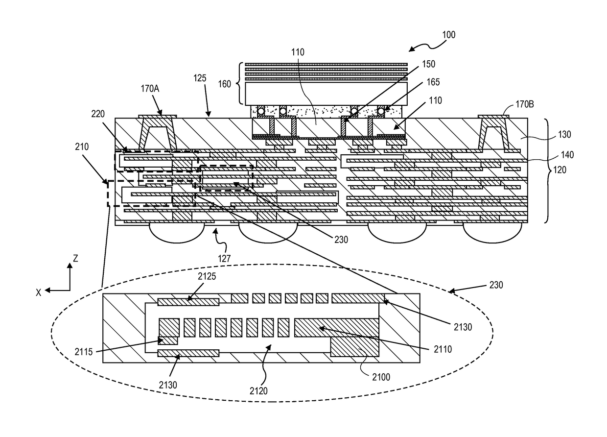
[0026]FIG. 1 shows a cross-sectional side view of a microelectronic package according to one embodiment. As illustrated in FIG. 1, microelectronic package 100 utilizes bumpless build-up layer (BBUL) technology. Microelectronic package 100 includes carrier 120 having surface 125 and opposing surface 127. Die 110, such as a microprocessor die, is embedded in carrier 120 at surface 125. In one embodiment, die 110 is a silicon die or the like having a thickness of approximately 150 micrometers (μm). In another example, die 110 can be a silicon die or the like that has a thickness less than 150 μm such as 50 μm to 150 μm. It is appreciated that other thicknesses for die 110 are possible.

[0027]Referring to FIG. 1, die 110 and carrier 120 are in direct physical contact with each other (e.g., there are no solder bumps connecting die 110 to carrier 120). Die 110 is directly connected to carrier 120 at its device side (device side down as viewed). Carrier 120 includes multiple build-up layers...


PUM

PropertyMeasurementUnit
thicknessaaaaaaaaaa
thicknessaaaaaaaaaa
thicknessaaaaaaaaaa

Abstract

An apparatus including a die including a first side and an opposite second side including a device side with contact points and lateral sidewalls defining a thickness of the die; a build-up carrier coupled to the second side of the die, the build-up carrier including a plurality of alternating layers of conductive material and insulating material, wherein at least one of the layers of conductive material is coupled to one of the contact points of the die; and at least one device within the build-up carrier disposed in an area void of a layer of patterned conductive material. A method and an apparatus including a computing device including a package including a microprocessor are also disclosed.

Description

CROSS-REFERENCE TO RELATED APPLICATION[0001]This patent application is a U.S. National Phase Application under 35 U.S.C. §371 of International Application No. PCT / US2011 / 068034, filed Dec. 30, 2011, entitled INTEGRATION OF LAMINATE MEMS IN BBUL CORELESS PACKAGE.BACKGROUND[0002]Field[0003]Packaging for microelectronic devices.[0004]Description of Related Art[0005]Microelectromechanical systems (MEMS) devices are a micro or nano device that integrates mechanical and electrical elements on a common substrate typically using microfabrication technology. The mechanical elements are fabricated using lithographic processes on a substrate, such as a silicon substrate, to selectively pattern the devices according to known techniques. Additional layers are often added to the substrates and then micromachined until the MEMS device is in a design configuration. MEMS devices include actuators, sensors, switches, accelerometers, modulators and optical devices (MEMS).[0006]Because a MEMS device ty...

Claims


Application Information

Patent Timeline
Patent Type & Authority Patents(United States)
IPC IPC(8): B81B7/02B81B7/00B81C1/00H01L23/00H05K1/18
CPCB81B7/0006B81C1/0023B81C1/00134H01L2924/1461H01L2924/15311H05K1/185H01L2224/97H01L2224/82H01L2924/10253H01L2924/00H01L2224/73204H01L2224/16225H01L2224/32225H01L2924/12042B81B2207/012B81B2207/07H01L24/24H01L24/82H01L2224/0401H01L2224/04105H01L2224/16135H01L2224/32245H01L2224/73259H01L2224/73267H01L2224/821H01L2224/82047H01L2224/92244H01L23/5389H01L23/48B81B7/0074B81B2201/0264B81B2201/038B81B2203/0315B81C1/00087B81C2203/019
Inventor TEH, WENG HONGSANKMAN, ROBERT L.
Owner INTEL CORP
Features
  • R&D
  • Intellectual Property
  • Life Sciences
  • Materials
  • Tech Scout
  • Unparalleled Data Quality
  • Higher Quality Content
  • 60% Fewer Hallucinations
Learn More