Sensor provided with metal oxide film and use thereof

a technology of metal oxide film and sensor, which is applied in the field of sensors including metal oxide film, can solve the problems of high fabrication cost, unsuitability for mass production, and complex process of optical sensors of patent literature 1, and achieve the effect of reducing the size and thickness of the sensor and low-cost fabrication of the sensor

Active Publication Date: 2017-07-18
ORMON CORP
View PDF43 Cites 0 Cited by
  • Summary
  • Abstract
  • Description
  • Claims
  • Application Information

AI Technical Summary

Benefits of technology

[0019]The optical sensor of Patent Literature 2 is a sensor fabricated by forming a single-layer film on a substrate. However, because the film is made of an amorphous semiconductor, the film is low in stability. Therefore, the optical sensor of Patent Literature 2 requires a heating element for ensuring the stability of the film. This causes the substrate to be always subjected to heat, thus causing a low degree of freedom of substrate selectivity. Further, the formation of the film by a vacuum process may result in unsuitability for mass production with a larger diameter and high fabrication cost.
[0042]This brings about an effect of achieving a multifunctional sensor capable of detecting light, hydrogen gas, and air pressure and allowing the sensor to detect a slight amount of light and hydrogen gas and a further effect of achieving reduction in size and thickness of the sensor and achieving low-cost fabrication of the sensor.

Problems solved by technology

However, the optical sensor of Patent Literature 1 inevitably takes the form of a multi-layered film because it is necessary to join a p-type semiconductor and an n-type semiconductor to each other in order to generate photovoltaic power.
Further, the optical sensor of Patent Literature 1 has a complex process because it requires formation of a multi-layered film on a transparent conductive film by a vacuum process with the films matched in condition to each other and also requires a resist, etching, etc.
Furthermore, the use of the vacuum process may result in unsuitability for mass production with a larger diameter, high fabrication cost, and difficulty of fabricating a sensor on a flexible substrate.
However, because the film is made of an amorphous semiconductor, the film is low in stability.
This causes the substrate to be always subjected to heat, thus causing a low degree of freedom of substrate selectivity.
Further, the formation of the film by a vacuum process may result in unsuitability for mass production with a larger diameter and high fabrication cost.
However, the optical irradiation position detection sensor of Patent Literature 3 requires a high-resistance film for increasing the accuracy of detection of a position irradiated with light, and a normal ITO film is too low in resistance, while it is difficult to increase the resistance.
Further, although it is necessary to reduce the film thickness in order to obtain a high-resistance film, the use of a film with a film thickness of several nanometers to several tens of nanometers in Patent Literature 3 makes it difficult to further reduce the film thickness, thus making it difficult to reduce the size and the thickness.
Further, the complicated structure may result in high fabrication cost and unsuitability for mass production with a larger diameter.

Method used


Image

  • Sensor provided with metal oxide film and use thereof
  • Sensor provided with metal oxide film and use thereof
  • Sensor provided with metal oxide film and use thereof

Examples


example 1

Preparation of a Primer Composition and Formation of an Organic Film

[0221]As a primer composition, a chemical solution was prepared by mixing 39% by weight of 2-acryloyloxyethyl-phthalic acid (commercially available as HOA-MPL from KYOEISHA CHEMICAL Co., Ltd.), 10% by weight of dimethylaminoethyl methacrylate (commercially available as DM from KYOEISHA CHEMICAL Co., Ltd.), 25% by weight of pentaerythritol acrylate (commercially available as PE-3A from KYOEISHA CHEMICAL Co., Ltd.), 25% by weight of diethyleneglycol dimethacrylate (commercially available as 2EG from KYOEISHA CHEMICAL Co., Ltd.), and 1% by weight of IRGACURE 1173 (manufactured by Ciba Specialty Chemicals, Inc.) as a polymerization reaction initiator so that the total was 100% by weight.

[0222]The 2-acryloyloxyethyl-phthalic acid was used as an addition polymerizable compound including an acid group. Dimethylaminoethyl methacrylate was used as an addition polymerizable compound including a basic group. Pentaerythritol ac...

example 2

Formation of a Metal Thin Film

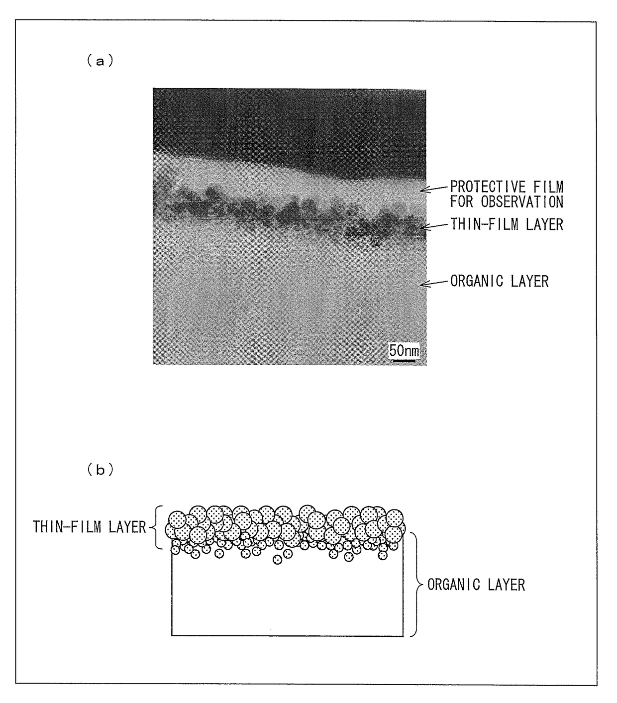
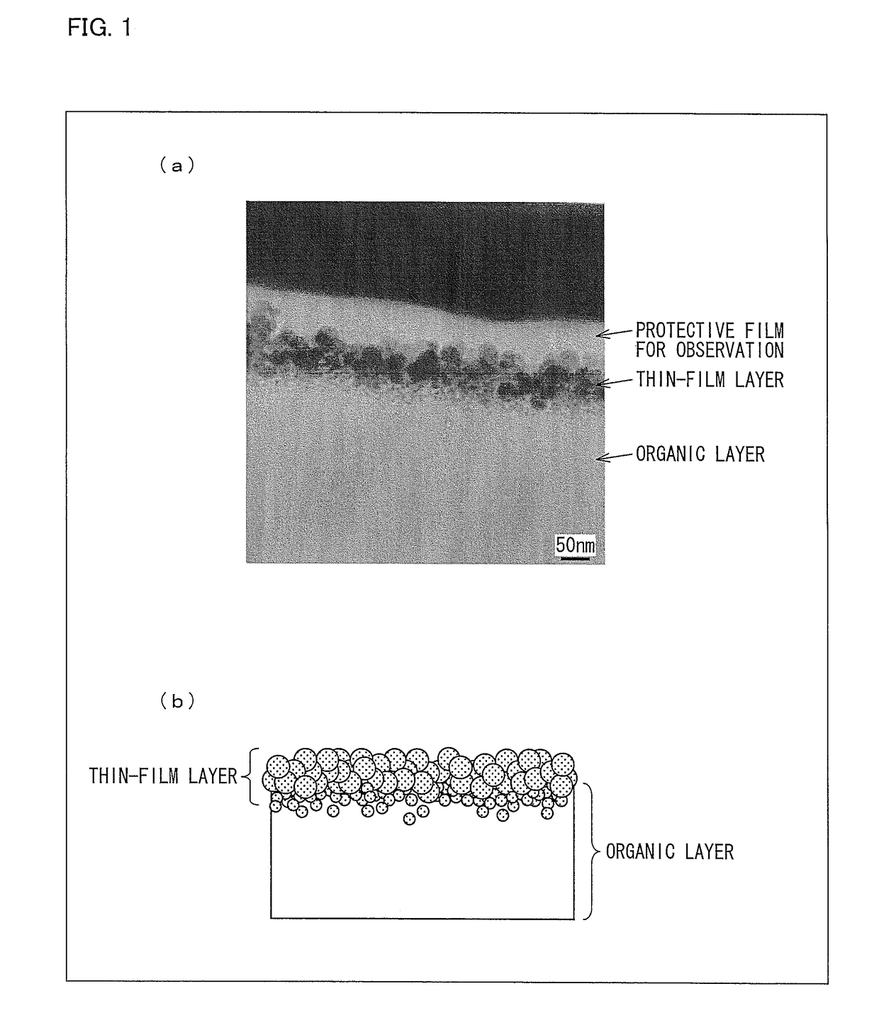
[0224]A metal thin film was obtained by subjecting, to the following steps, the acrylic sheet on which the organic film had been formed.

(1) The acrylic sheet was immersed in an 8 M aqueous solution of potassium hydroxide at 60° C. and kept there for 2 minutes.

(2) The acrylic sheet was washed thoroughly in distilled water.

[0225](3) The acrylic sheet was immersed in an aqueous solution of metal ions at room temperature and kept there for 10 minutes. The aqueous solution of metal ions was obtained by mixing together a 100 mM aqueous solution of indium chloride and a 100 mM aqueous solution of sodium acetate with a volume ratio of 1:1.

(4) The acrylic sheet was washed thoroughly in distilled water.

(5) The metal ions were reduced by immersing the acrylic sheet in a 100 mM aqueous solution of sodium borohydride at 40° C. and keeping it there for 10 minutes.

(6) The acrylic sheet was washed thoroughly in distilled water.

(7) The acrylic sheet was dried in a nitro...

example 3

Fabrication of a Sensor and Detection of Light Irradiation by the Sensor

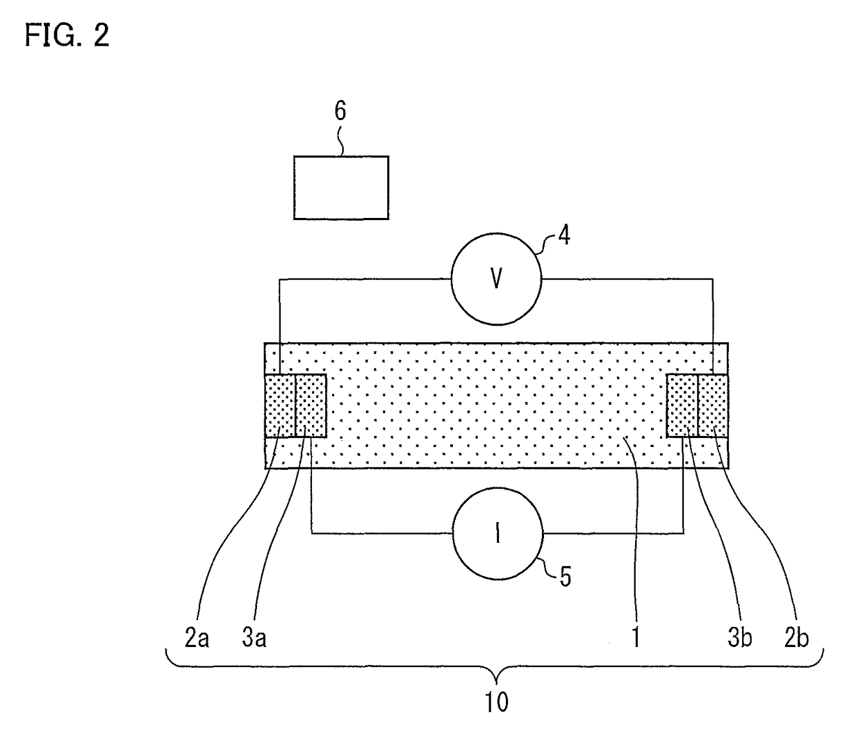
[0231]A circuit which has two outer terminals connected to a power supply and which can detect an electric potential difference with two inner terminals was formed by wiring the four terminals with a conductive paste at both ends of the element. FIG. 2 is a schematic view of the appearance of a sensor 10 according to an embodiment of the present invention thus fabricated. In FIG. 2, the reference sign 1 denotes an element including an organic film or an indium oxide film, the reference signs 2a and 2b denote outer terminals, the reference signs 3a and 3b denote inner terminals, the reference sign 4 denotes a voltmeter, the reference sign 5 denotes an ammeter, and the reference sign 6 denotes a light source. The sensor 10 according to one or more embodiments of the present invention includes the element 1, the outer terminals 2a and 2b, and the inner terminals 3a and 3b. It should be noted that in this specificat...


PUM

PropertyMeasurementUnit
particle diameteraaaaaaaaaa
temperatureaaaaaaaaaa
thicknessaaaaaaaaaa

Abstract

A sensor capable of detecting light, hydrogen gas, and air pressure includes a metal oxide film produced by a process including the steps of: (a) forming an organic film by using a primer composition containing (i) an addition polymerizable compound including three or more reactive groups, (ii) an addition polymerizable compound including an acid group, and (iii) an addition polymerizable compound including a hydrophilic functional group; (b) forming a metal (M1) salt from the acid group; (c) substituting the metal (M1) salt of the acid group with a metal (M2) salt by treating the organic film with a metal (M2) ion aqueous solution; (d) reducing the metal (M2) ion so that a metal film is formed on a surface of the organic film; and (e) oxidizing the metal film.

Description

BACKGROUND[0001]Technical Field[0002]The present invention relates to a sensor including a metal oxide film and use thereof and, more specifically, to a sensor including a metal oxide film formed by wet processing and capable of detecting light, hydrogen gas, and air pressure, a method for fabricating such a sensor, and a method for detecting a concentration of hydrogen gas etc. by using such a sensor.[0003]Related Art[0004]Optical sensors are widely used for optical communications compliant with IrDA (Infrared Data Association) etc., such as television and audio infrared remote controllers, office automation equipment, industrial equipment, consumer equipment, etc.[0005]Further, hydrogen gas has drawn attention as clean and recyclable energy. However, hydrogen gas is known to be highly explosive. Therefore, in order for hydrogen gas to be widely used as a source of energy in the future, it is critical to take safety measures to safely utilize a system. As a tool that contributes to...

Claims


Application Information

Patent Timeline
Patent Type & Authority Patents(United States)
IPC IPC(8): B32B15/08G01N33/00G01L11/02G01L9/02B32B15/04G01N27/04H01L31/0248G01N27/12
CPCH01L31/0248G01L9/02G01L11/02G01N27/126G01N33/005
Inventor OHMAE, KEISUKEMORI, TETSUYAHAYASE, TETSUONAKAJIMA, SEIJINISHIGUCHI, MARIKO
Owner ORMON CORP
Why Eureka
Try Eureka