Magnetic sensor having a recessed die pad

a magnetic converging plate and die pad technology, applied in the field of magnetic sensors, can solve the problems of increasing the number of processes, difficulty in achieving the magnetic converging plate having high magnetic permeability and low coercive force, etc., and achieves the effect of suppressing an increase in the number of work processes, small variation in position, and high magnetic permeability

Active Publication Date: 2017-08-22
ABLIC INC
View PDF9 Cites 1 Cited by
  • Summary
  • Abstract
  • Description
  • Claims
  • Application Information

AI Technical Summary

Benefits of technology

[0017]It is an object of the present invention to provide a magnetic sensor and a method of manufacturing the magnetic sensor capable of arranging a magnetic converging plate on a substrate on which Hall elements and a circuit are formed, with a small variation in position while suppressing an increase in number of work processes, the magnetic converging plate having high magnetic permeability and low coercive force.
[0020]With the use of the above-mentioned measure, it is possible to suppress a variation in position of the magnetic converging plate, reducing the variation in magnetic property. Further, since the magnetic converging plate holder for adjusting the position of the magnetic converging plate is formed in the die pad of the package, additional manufacturing process is needed, suppressing the manufacturing cost. Further, since the magnetic converging plate and the circuit are manufactured in the different processes, high-temperature heat treatment can be performed after a magnetic film is formed. Consequently, the magnetic converging plate having high magnetic permeability and low coercive force can be manufactured, and a magnetic sensor having higher sensitivity and higher accuracy can thus be realized.

Problems solved by technology

However, since annealing at such high temperature cannot be applied to the magnetic converging plate after the circuit and the Hall elements are formed, it is difficult to attain the magnetic converging plate having high magnetic permeability and low coercive force.
Further, the method involving arranging the structure for adjusting the position of the magnetic converging plate has a drawback that the number of processes increases due to additional processes such as forming the structure for position adjustment and removing the structure after the magnetic converging plate is arranged.

Method used


Image

  • Magnetic sensor having a recessed die pad
  • Magnetic sensor having a recessed die pad
  • Magnetic sensor having a recessed die pad

Examples


Embodiment Construction

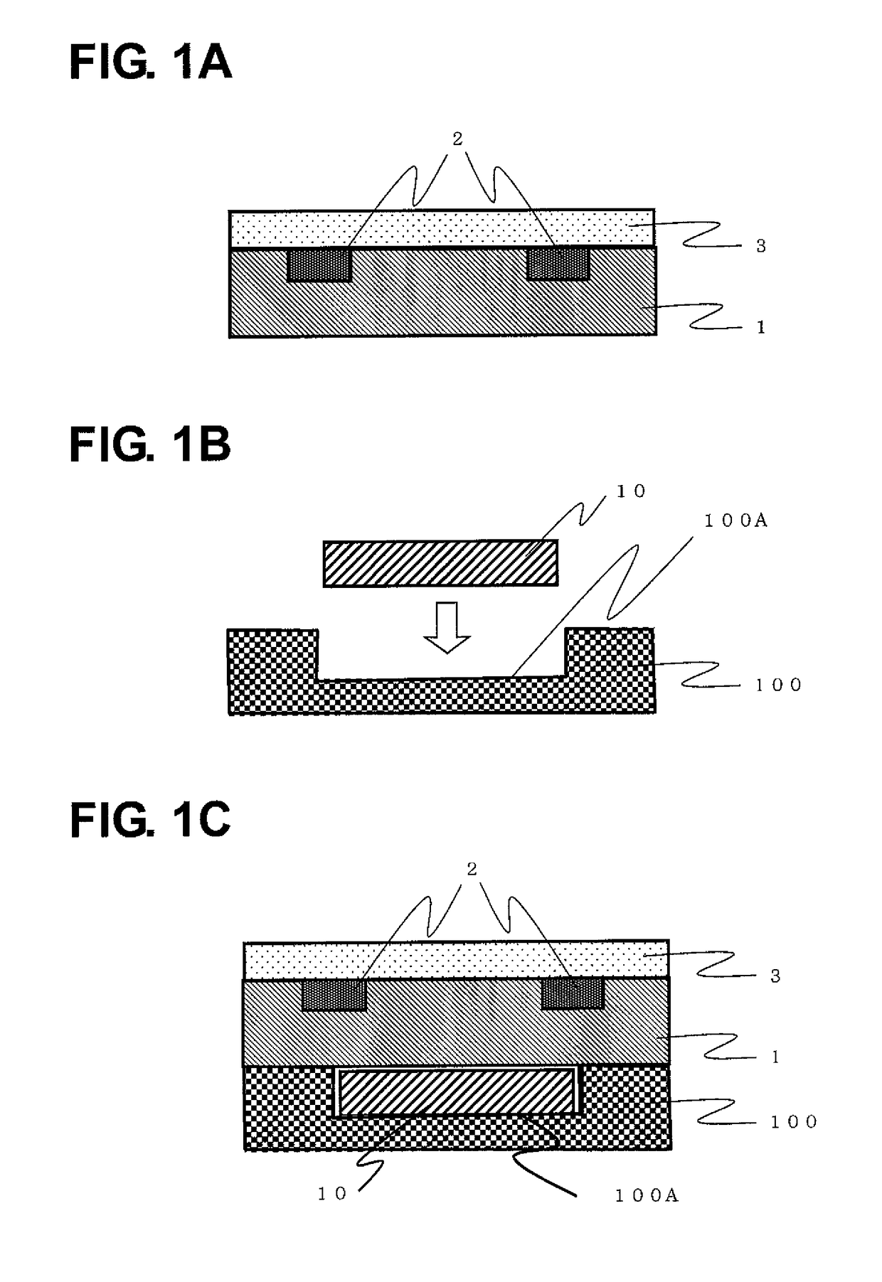
[0025]A detailed description is now given of an embodiment of the present invention with reference to the drawings.

[0026]FIG. 1A to FIG. 1C are sectional views relating to a method of manufacturing a magnetic sensor according to the embodiment of the present invention.

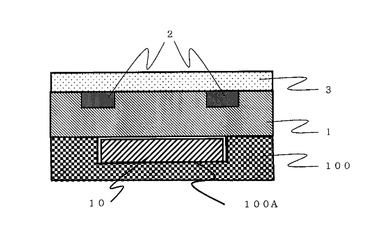
[0027]First, as illustrated in FIG. 1A, a semiconductor circuit that forms a magnetic sensor having Hall elements 2 is formed on a P-type semiconductor substrate 1 through a normal semiconductor manufacturing process. The Hall element 2 is a horizontal Hall element having a square or cross-shaped vertical magnetic field sensing portion having a four-fold rotational axis, and, at respective vertices and end portions thereof, vertical magnetic field detection control current input terminals and vertical magnetic field Hall voltage output terminals corresponding to surface N-type highly-doped regions having the same shape. At least one pair of the Hall elements 2 is formed on a surface of the semiconductor substrate 1. No...


PUM


Abstract

A magnetic sensor has a pair of Hall elements formed in spaced-apart relationship on a front surface of a semiconductor substrate. A die pad is bonded to a back surface of the semiconductor substrate and overlaps the Hall elements. The die pad has formed therein a magnetic converging plate holder having a recessed portion, and a magnetic converging plate having the same shape and size as the recessed portion is fitted in the recessed portion of the magnetic converging plate holder.

Description

BACKGROUND OF THE INVENTION[0001]1. Field of the Invention[0002]The present invention relates to a magnetic sensor that includes a magnetic converging plate and is configured to detect magnetic fields in a vertical direction and a horizontal direction, and to a method of manufacturing the magnetic sensor.[0003]2. Description of the Related Art[0004]Hall elements allow non-contact position detection and non-contact angle detection as magnetic sensors, and are thus often used in various applications.[0005]First, the principle of magnetic detection with the Hall elements is described. When a magnetic field is applied vertically to a current flowing through a substance, an electric field (Hall voltage) is generated in a direction vertical to both the current and the magnetic field. Thus, the typical Hall elements are configured to detect a vertical magnetic field component with a current caused to flow on a surface of a substrate (wafer).[0006]In addition, it is known that the Hall elem...

Claims


Application Information

Patent Timeline
Patent Type & Authority Patents(United States)
IPC IPC(8): H01L43/04H01L43/14G01R33/00G01R33/07H01L43/06
CPCH01L43/04G01R33/0052G01R33/07H01L43/065H01L43/14H03K19/18H03K17/9517G01R15/202G01R15/207G01R33/077G01D5/145H04Q2213/307H02K11/215G01R21/08G01R33/072H01L23/32H01L23/13G01R33/0206H01L23/145H01L23/15G01R33/0005H10N52/01H10N52/80H10N52/101
Inventor HIOKA, TAKAAKIEBIHARA, MIKA
Owner ABLIC INC
Why Eureka
Try Eureka