Method for manufacturing LTPS TFT substrate structure and structure of LTPS TFT substrate

a technology of thin film transistor and substrate, which is applied in the field of display technology, can solve the problems of poor image quality, ineffective control of grain homogeneity and grain size, and in the field of ela crystallization techniques, and achieve the effects of speeding up the cooling rate of amorphous silicon, improving consistency and homogeneity, and enhancing the electrical property of driving

Active Publication Date: 2017-09-12
TCL CHINA STAR OPTOELECTRONICS TECH CO LTD
View PDF2 Cites 0 Cited by
  • Summary
  • Abstract
  • Description
  • Claims
  • Application Information

AI Technical Summary

Benefits of technology

[0008]An object of the present invention is to provide a method for manufacturing a low-temperature polycrystalline silicon (LTPS) thin-film transistor (TFT) substrate structure, which provides improved consistency of grain sizes of polycrystalline silicon in a driving TFT area and makes the grain sizes relatively large to ensure consistency of electrical property of the driving TFT.
[0009]Another object of the present invention is to provide a structure of a LTPS TFT substrate, which has improved consistency of grain sizes of polycrystalline silicon in a driving TFT area and makes the grain sizes relatively large to ensure consistency of electrical property of the driving TFT.
[0038]The efficacy of the present invention is that the present invention provides a method for manufacturing an LTPS TFT substrate structure, wherein patterns of a thermally conductive electrical-insulation layer that are of the same size are regularly distributed under a buffer layer of a driving TFT area so that in a subsequent crystallization process of an amorphous silicon layer resulting from ELA treatment, the thermally conductive electrical-insulation layer would absorb heat to speed up the cooling rate of the amorphous silicon to form crystal nuclei that gradually grow up during the annealing process. Since the thermally conductive electrical-insulation layer is made up of regularly distributed and size-consistent patterns, crystal grains of a polycrystalline silicon layer located in the driving TFT area show improved consistency and homogeneity and the grain sizes are relatively large to ensure the consistency of electrical property of the driving TFT, enhancing stability of electrical property of the driving TFT and preventing the events of poor image quality. The present invention provides an LTPS TFT substrate structure, wherein patterns of a thermally conductive electrical-insulation layer that are regularly distributed and have the same size are arranged under a buffer layer of a driving TFT area, so that crystal grains of a polycrystalline silicon layer located in the driving TFT area show improved consistency and homogeneity and the grain sizes are relatively large and thus, the electrical property of the driving TFT is consistent and electrical stability is improved.

Problems solved by technology

However, the state-of-the-art ELA crystallization techniques do not provide an effective control of grain homogeneity and grain size.
Consequently, the crystallization shows poor distribution over the entire substrate, leading to poor consistency of polycrystalline silicon grains in the area associated with the driving TFT and relatively small grain sizes, making the consistency and stability of electrical property of the driving TFT.
As such, poor image quality may readily occur.

Method used


Image

  • Method for manufacturing LTPS TFT substrate structure and structure of LTPS TFT substrate
  • Method for manufacturing LTPS TFT substrate structure and structure of LTPS TFT substrate
  • Method for manufacturing LTPS TFT substrate structure and structure of LTPS TFT substrate

Examples


Embodiment Construction

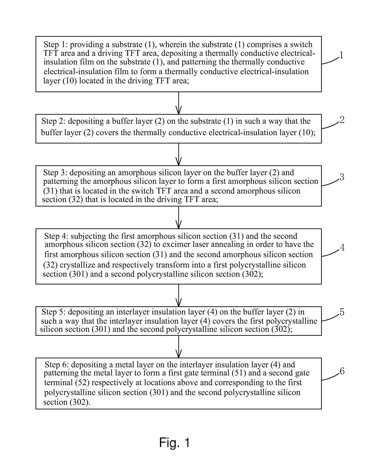
[0047]To further expound the technical solution adopted in the present invention and the advantages thereof, a detailed description is given to a preferred embodiment of the present invention and the attached drawings.

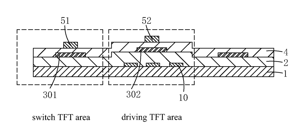
[0048]Referring to FIG. 1, firstly, the present invention provides a method for manufacturing a low-temperature polycrystalline silicon (LTPS) thin-film transistor (TFT) substrate structure, which comprises the following steps:

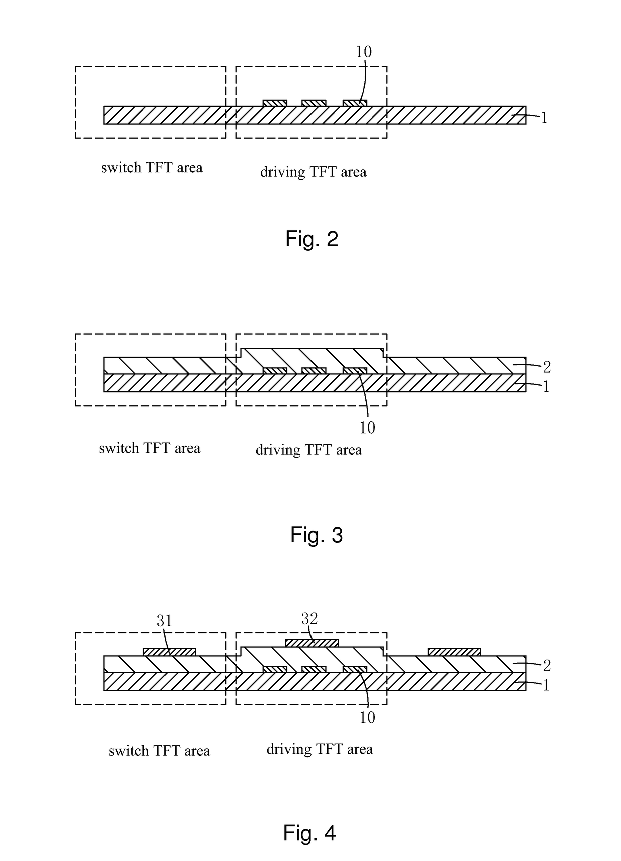
[0049]Step 1: as shown in FIG. 2, providing a substrate 1, wherein the substrate 1 comprises a switch TFT area and a driving TFT area, depositing a thermally conductive electrical-insulation film on the substrate 1, and patterning the thermally conductive electrical-insulation film to form a thermally conductive electrical-insulation layer 10 located in the driving TFT area.

[0050]Specifically, the substrate 1 can be a glass substrate or a silicon substrate.

[0051]Specifically, the thermally conductive electrical-insulation layer 10 is formed of a ...


PUM

PropertyMeasurementUnit
thermally conductive electrical-insulationaaaaaaaaaa
thermally conductiveaaaaaaaaaa
thermally conductive electrical-aaaaaaaaaa

Abstract

The present invention provides a method for manufacturing an LTPS TFT substrate structure and a structure of an LTPS TFT substrate. The method for manufacturing the LTPS TFT substrate structure according to the present invention provides patterns of a thermally conductive electrical-insulation layer that are of the same size and regularly distributed under a buffer layer of a driving TFT area to absorb heat in a subsequent excimer laser annealing process so as to speed up the cooling rate of amorphous silicon to form crystal nuclei that gradually grow up in the annealing process. Since the thermally conductive electrical-insulation layer is made up of regularly distributed and size-consistent patterns, crystal grains of a polycrystalline silicon layer located in the driving TFT area show improved consistency and homogeneity and the grain sizes are relatively large to ensure the consistency of electrical property of the driving TFT. The structure of the LTPS TFT substrate structure according to the present invention includes patterns of a thermally conductive electrical-insulation layer that are regularly distributed under a buffer layer of a driving TFT area and have the same size, so that crystal grains of a polycrystalline silicon layer located in the driving TFT area show improved consistency and homogeneity and the grain sizes are relatively large and thus, the electrical property of the driving TFT is consistent.

Description

BACKGROUND OF THE INVENTION[0001]1. Field of the Invention[0002]The present invention relates to the field of display technology, and in particular to a method for manufacturing a low-temperature polycrystalline silicon (LTPS) thin-film-transistor (TFT) substrate structure and a structure of a LTPS TFT substrate.[0003]2. The Related Arts[0004]LTPS TFT has valuable and potential uses in the field of high definition display devices of active matrix liquid crystal display (AMLCD) and active matrix organic light emitting diode (AMOLCD).[0005]Compared to the amorphous silicon (a-Si) technology, LTPS TFT has a relatively high mobility and excellent device stability. The mobility of LTPS TFT may be as high as tens to hundreds cm2 / Vs, which satisfy the needs of high-definition AMLCD and AMOLED displays. Thus, a LTPS display has a faster response speed and shows various advantages including high brightness, high resolution, and low power consumption. In addition to being used as a pixel swit...

Claims


Application Information

Patent Timeline
Patent Type & Authority Patents(United States)
IPC IPC(8): H01L21/02H01L27/12
CPCH01L21/02667H01L21/0262H01L21/02532H01L21/02592H01L21/02672H01L21/02675H01L27/1262H01L27/1274H01L27/1281H01L27/1285H01L27/1218H01L27/1296H01L27/1229
Inventor ZHANG, LIANGFEN
Owner TCL CHINA STAR OPTOELECTRONICS TECH CO LTD
Why Eureka
Try Eureka