Semiconductor device and semiconductor device manufacturing method

a semiconductor device and semiconductor technology, applied in semiconductor devices, semiconductor/solid-state device details, electrical apparatus, etc., can solve the problems of supporting members contacting the bump electrodes and damage the bump electrodes, so as to prevent cracking and chipping, reduce the number of manufacturing processes, and prevent damage to the projecting electrodes

Active Publication Date: 2017-11-07
LAPIS SEMICON CO LTD
View PDF2 Cites 0 Cited by
  • Summary
  • Abstract
  • Description
  • Claims
  • Application Information

AI Technical Summary

Benefits of technology

[0008]The present disclosure provides a semiconductor device that may prevent cracking and chipping at a peripheral portion of a substrate, and that may prevent damage to projecting electrodes.
[0009]Moreover, the present disclosure provides a semiconductor device manufacturing method that may reduce the number of manufacturing processes, prevent damage such as cracking and chipping of a substrate when a back face of the substrate is ground, and may achieve a thinner substrate.
[0012]According to the above first aspect, the present disclosure may provide a semiconductor device that may prevent cracking and chipping at a peripheral portion of a substrate, and that may prevent damage to projecting electrodes.
[0013]According to the above second aspect, the present disclosure may provide a semiconductor device manufacturing method that may reduce the number of manufacturing processes, prevent damage such as cracking and chipping of a substrate when a back face of the substrate is ground, and may achieve a thinner substrate.

Problems solved by technology

When the support member is being applied, there is a possibility that the support member could contact the bump electrodes and damage the bump electrodes.

Method used


Image

  • Semiconductor device and semiconductor device manufacturing method
  • Semiconductor device and semiconductor device manufacturing method
  • Semiconductor device and semiconductor device manufacturing method

Examples


first exemplary embodiment

[0035]Explanation follows regarding a semiconductor device and a semiconductor device manufacturing method according to a first exemplary embodiment of the present disclosure, with reference to FIG. 1 to FIG. 18. Here, an example is described in which the semiconductor device and the semiconductor device manufacturing method according to the first exemplary embodiment are applied to a semiconductor device and a manufacturing method thereof with a wafer level chip size package structure.

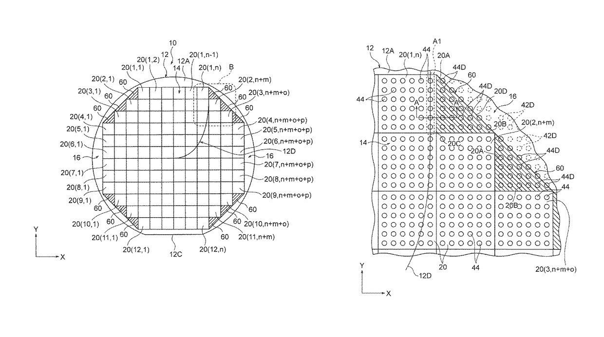
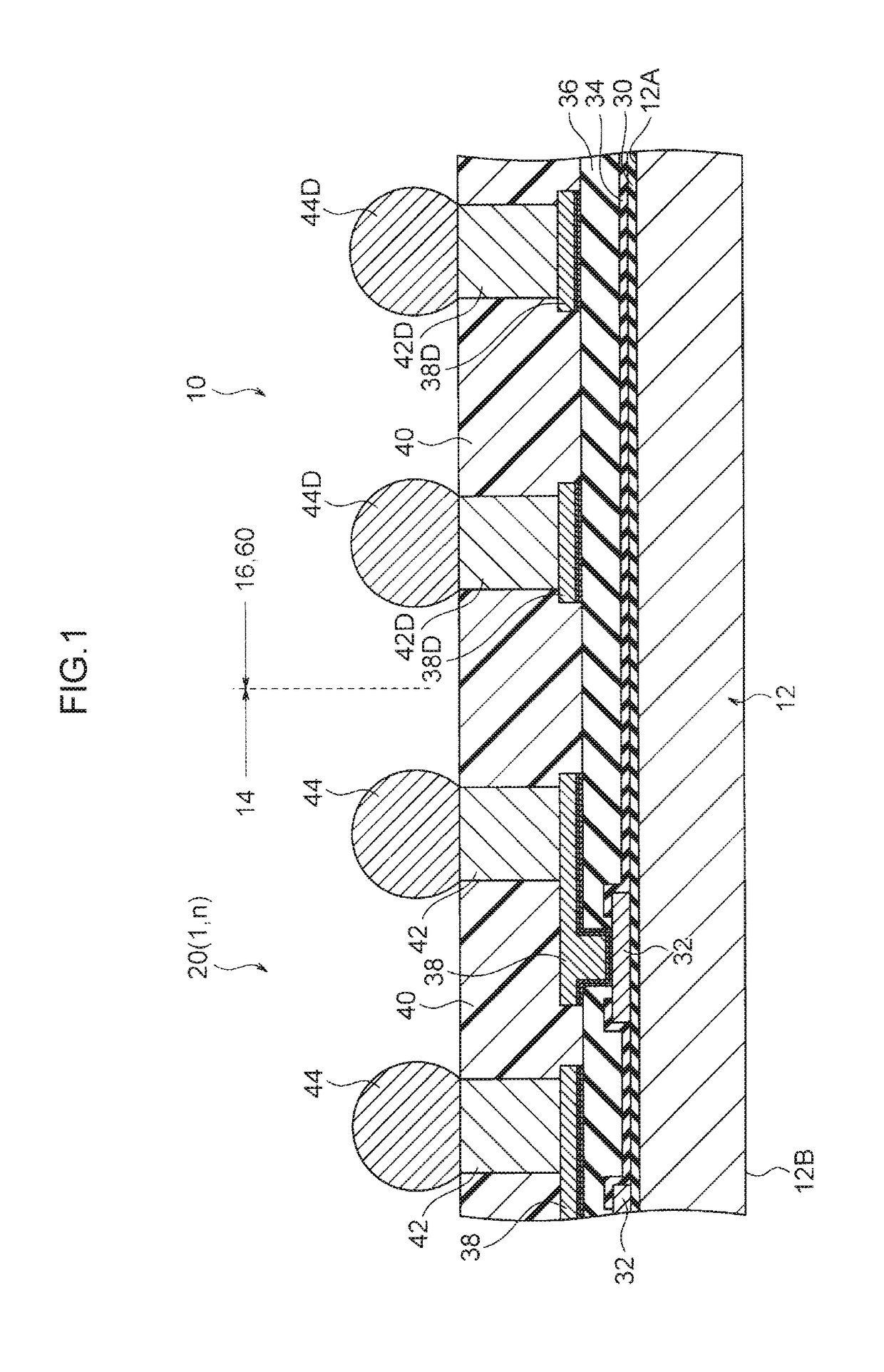
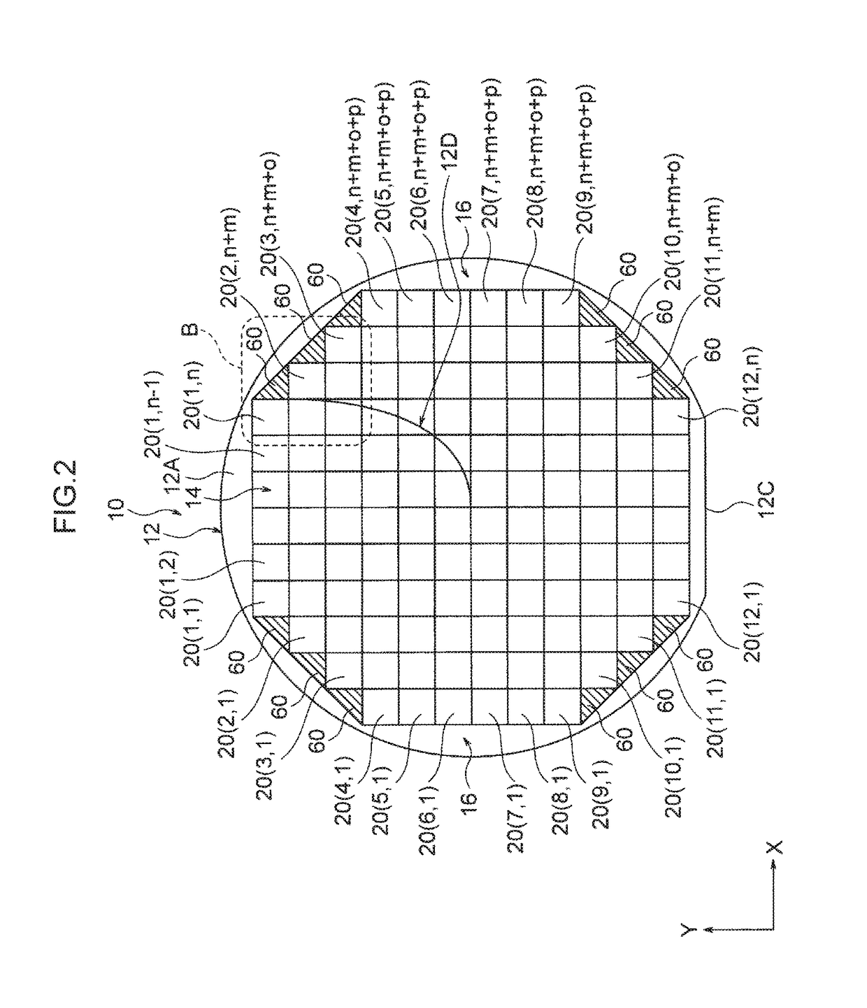
[0036]As illustrated in FIG. 1 to FIG. 3, a semiconductor device 10 according to the present exemplary embodiment includes a semiconductor wafer 12, serving as a substrate. In the present exemplary embodiment, a silicon single crystal wafer is employed as the semiconductor wafer 12. As illustrated in FIG. 2, in plan view, the semiconductor wafer 12 is formed in a circular shape. A portion of the circumference of the semiconductor wafer 12 (at the bottom side in FIG. 2) is formed with an orientation fl...

second exemplary embodiment

[0079]Explanation follows regarding a semiconductor device 10 and a semiconductor device manufacturing method according to a second exemplary embodiment of the present disclosure, with reference to FIG. 19.

[0080]As illustrated in FIG. 19, in the semiconductor device 10 according to the present exemplary embodiment, the dummy electrode pads 42D are not arrayed in the peripheral portion 16 of the main face 12A of the semiconductor wafer 12 in the regions that do not overlap the triangles 60. A front face of the sealing resin layer 40 (see FIG. 1) is exposed in these regions. Note that, in the present exemplary embodiment, the dummy redistribution lines 38D (see FIG. 1) may or may not be arrayed below the dummy electrode pads 42D. Configurations other than that of the dummy electrode pads 42D are similar to those of the semiconductor device 10 and the semiconductor device manufacturing method according to the first exemplary embodiment.

[0081]Accordingly, the semiconductor device 10 and...


PUM


Abstract

The present disclosure provides a semiconductor device including: a substrate including, in a central portion the substrate, n first element formation regions having a rectangular shape and are arrayed along a first direction, and n+m second element formation regions arrayed along the first direction adjacent to the first element formation regions; plural projecting electrodes formed at each of the first and the second element formation regions; and plural dummy projecting electrodes formed, at a peripheral portion, overlapping a triangle defined by a first edge of the first element formation region that forms a boundary between the first element formation region and the peripheral portion, and a second edge of the second element formation region that is adjacent to a corner of the first edge and that forms a boundary between the second element formation region and the peripheral portion.

Description

CROSS-REFERENCE TO RELATED APPLICATION[0001]This application is based on and claims priority under 35 USC 119 from Japanese Patent Application No. 2015-190200 filed on Sep. 28, 2015, the disclosure of which is incorporated by reference herein.BACKGROUND[0002]Technical Field[0003]The present disclosure relates to a semiconductor device and a semiconductor device manufacturing method.[0004]Related Art[0005]Japanese Patent Application Laid-Open (JP-A) No. 2004-288725 discloses a manufacturing method for a semiconductor device in a Wafer Level Chip Size Package (WL-CSP). In this semiconductor device manufacturing method, first, an IC wafer is formed with bump electrodes arrayed on an active face (front face), and a support member is applied to a peripheral edge portion of the active face of the IC wafer. Moreover, a protective tape used during back grinding is applied over the support member, so as to cover the bump electrodes. In a state in which the active face is protected by the pro...

Claims


Application Information

Patent Timeline
Patent Type & Authority Patents(United States)
IPC IPC(8): H01L23/544H01L23/00
CPCH01L24/14H01L24/11H01L2224/11002H01L2224/1412H01L2224/1184H01L2224/1401H01L2224/11009H01L21/4853H01L23/49838H01L2224/05569H01L23/585H01L24/02H01L24/03H01L24/05H01L24/13H01L24/94H01L2221/68327H01L2221/6834H01L2224/02313H01L2224/02331H01L2224/0239H01L2224/03462H01L2224/0347H01L2224/0391H01L2224/05083H01L2224/05147H01L2224/05166H01L2224/05647H01L2224/131H01L2224/13147H01L2224/94H01L2224/02311H01L21/6836H01L2221/68381H01L2924/014H01L2924/00014H01L2224/11H01L2924/01022H01L2924/01029
Inventor SAITO, HIROKAZU
Owner LAPIS SEMICON CO LTD
Why Eureka
Try Eureka