
Systems and methods for a high performance memory cell structure

Inactive Publication Date: 2017-11-28
MARVELL ASIA PTE LTD
View PDF3 Cites 0 Cited by
  • Summary
  • Abstract
  • Description
  • Claims
  • Application Information

AI Technical Summary

Benefits of technology

The patent text discusses various technical effects to improve the performance of a memory device. In one implementation, the transistors in the memory device are designed to be stronger than certain components to ensure disturb stability. Another implementation includes separating certain components to reduce fight between them and improve performance. Additionally, a differential read structure is used for improved performance. Overall, these technical effects enhance the speed, reliability, and performance of the memory device.

Problems solved by technology

In advanced semiconductor process nodes, the performance-area trade-off may incur performance drawbacks that affect yield and reliability of the memory unit.
Thus the performance-area trade-off can be significant.
However, a SR2P may be susceptible to interactions between the two ports, and write-induced-read failures, read-induced-write failures read-induced-read failures, and both-ports-ON-induced disturb failures.
For multi-port memory cells, maintaining a good write / read / stability margin can be difficult, which may result in larger size of individual transistors, a greater overall leakage power, and greater risk of port-to-port interaction related failures.

Method used


Image

  • Systems and methods for a high performance memory cell structure
  • Systems and methods for a high performance memory cell structure
  • Systems and methods for a high performance memory cell structure

Examples


Embodiment Construction

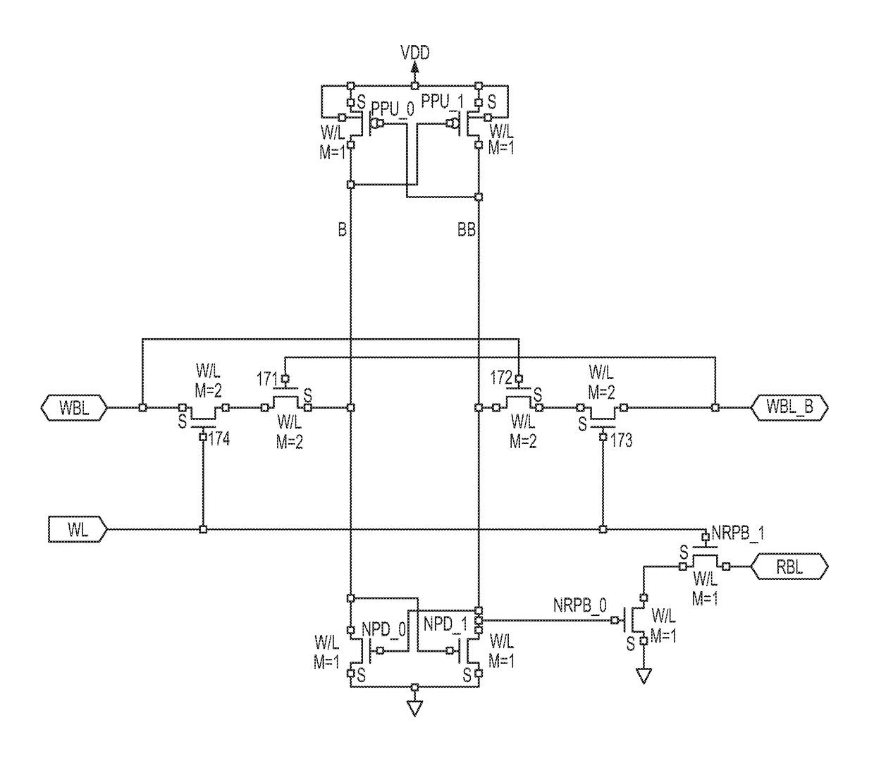
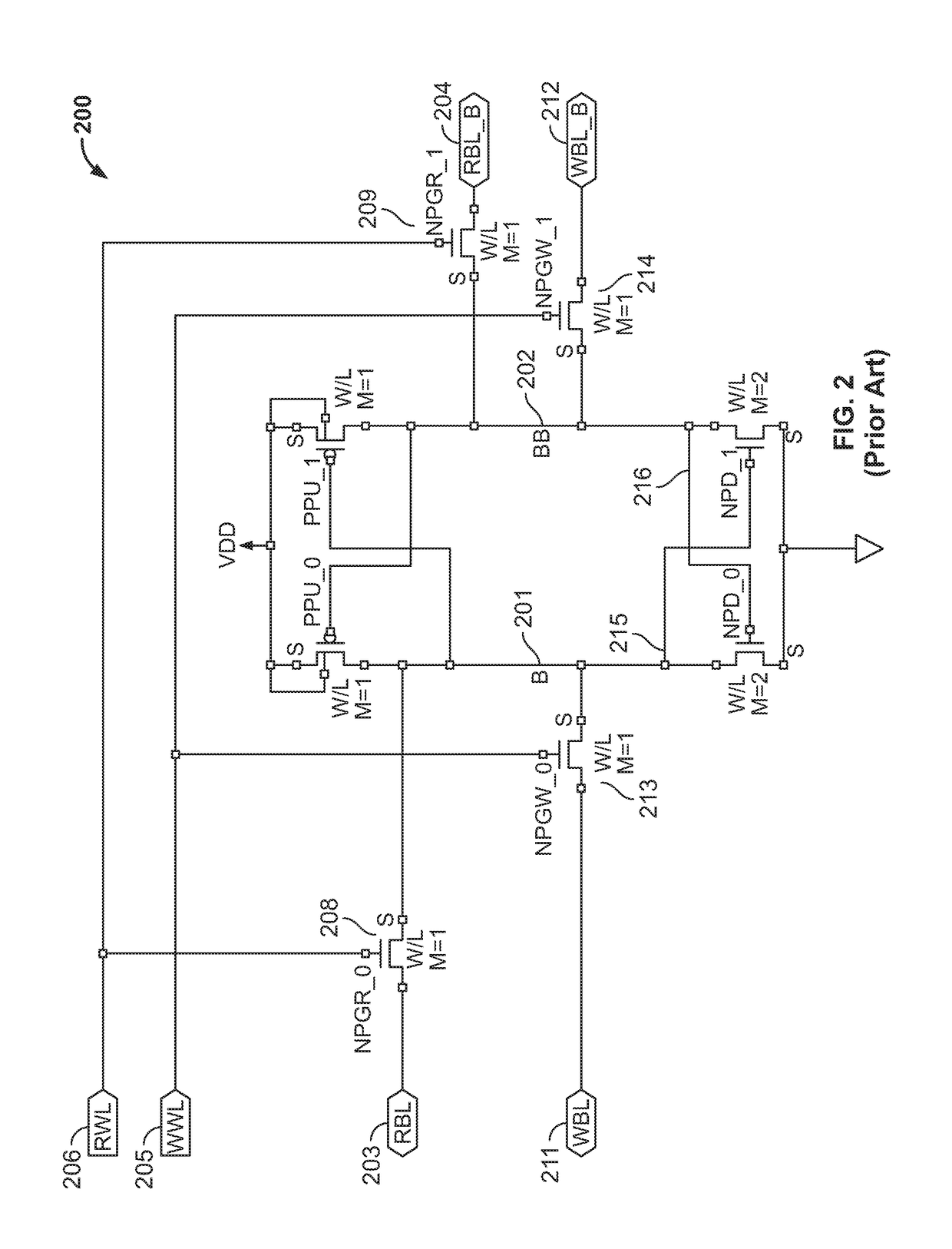
[0030]This disclosure describes methods and systems for a 1-read / 1-write high performance SRAM cell having a structure that is immune to read-write interactions that may diminish performance or cause intermittent, difficult-to-detect memory failures. The memory cell structure reduces port-to-port interactions such as read-to-write interactions, write-to-read interactions, read-to-read interactions, multiple-port-ON-disturb, such that the memory cell can be scaled to multi-port cells without sacrificing robustness of the cell.

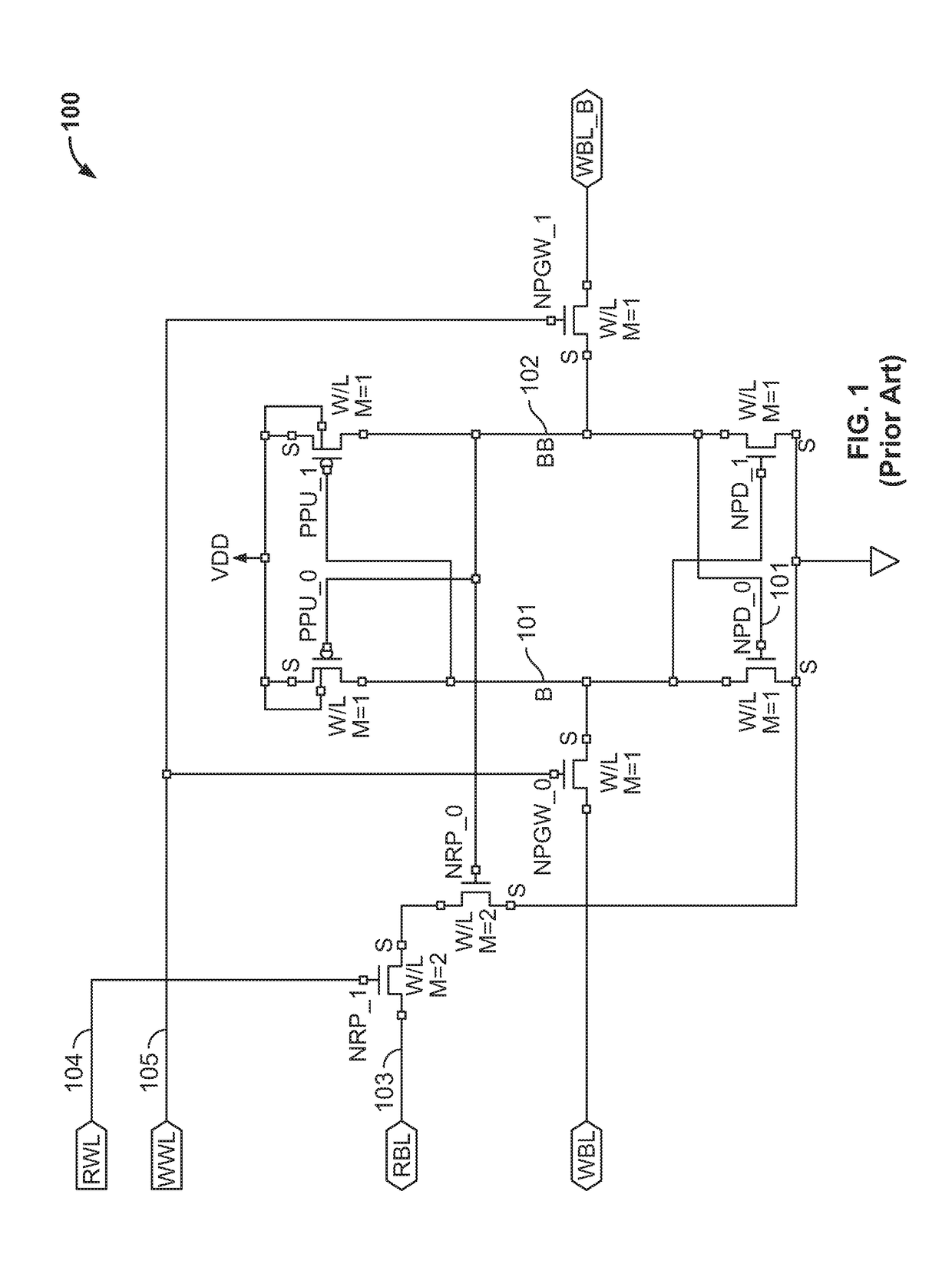
[0031]FIG. 1 provides an exemplary block diagram illustrating an 8T single-ended-read cell, which is immune to read-write interactions, with a smaller area but lower performance. The memory cell structure 100 is immune to read-write interactions because the two internal nodes of the cell, B 101 and BB 102 are de-coupled from read bit-line 103 (RBL). If a write operation and a read operation happen at the same time, both the read word-line 104 (RWL) and the write...


PUM


Abstract

Systems and methods described herein provide a memory cell circuit. The memory cell circuit includes a first internal node communicatively coupled to a first write bit line via a first write pass gate, and a second internal node communicatively coupled to a second write bit line via a second write pass gate. The memory cell circuit further includes a first read bit line connected to a first read pass gate and a first transistor, and a second read bit line connected to a second read pass gate and a second transistor. The first internal node is decoupled from the first read bit line by the first transistor, and the second internal node is decoupled from the second read bit line by the second transistor when a write operation and a read operation occur at the same time.

Description

CROSS-REFERENCE TO RELATED APPLICATIONS[0001]This disclosure claims the benefit of U.S. Provisional Patent Application No. 62 / 156,085, filed May 1, 2015, and U.S. Provisional Patent Application No. 62 / 174,141, filed Jun. 11, 2015. The aforementioned applications are hereby incorporated by reference herein in their entirety.FIELD OF USE[0002]This disclosure relates to a high performance 1-read / 1-write (2-port) memory cell structure.BACKGROUND OF THE DISCLOSURE[0003]The background description provided herein is for the purpose of generally presenting the context of the disclosure. Work of the inventors hereof, to the extent the work is described in this background section, as well as aspects of the description that may not otherwise qualify as prior art at the time of filing, are neither expressly nor impliedly admitted to be prior art against the present disclosure.[0004]Data memory elements such as static random-access memory (SRAM) can use two types of 1-Read / 1-Write memory bit cel...

Claims


Application Information

Patent Timeline
IPC IPC(8): G11C7/10G11C11/419G11C7/22
CPCG11C11/419G11C7/1051G11C7/22G11C7/1078G11C8/16G11C11/418
Inventor LEE, PETERLEE, WINSTON
Owner MARVELL ASIA PTE LTD
Learn More