

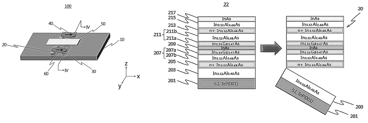
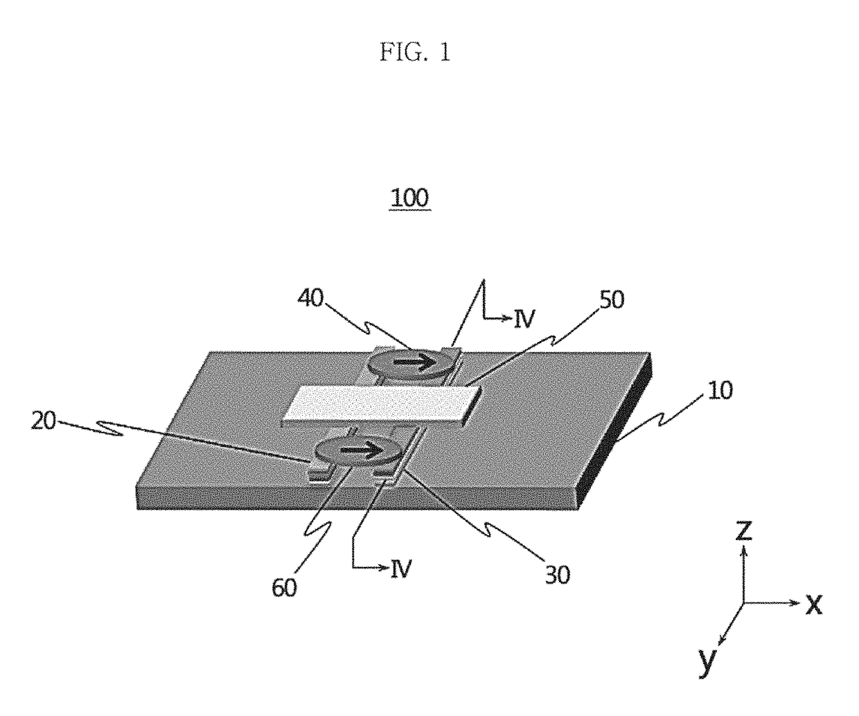
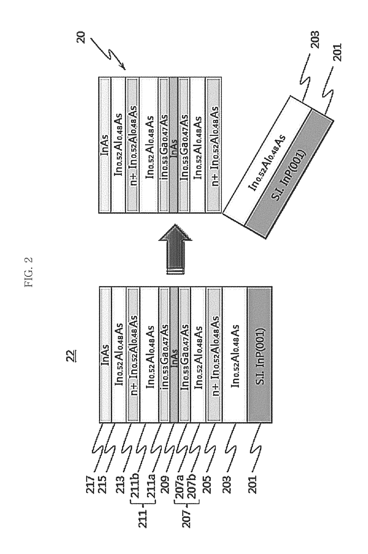
Complementary logic device using spin-orbit interaction difference and method for manufacturing the same
a technology of complementary logic and spin-orbit interaction, which is applied in the direction of semiconductor devices, digital storage, instruments, etc., can solve the problems of inability to fabricate 2deg or 2dhg structures with different spin-orbit interaction constants on a single substrate, and the limitation of reducing the size of the existing silicon-based complementary transistor
- Summary
- Abstract
- Description
- Claims
- Application Information
AI Technical Summary
Benefits of technology
Problems solved by technology
Method used
Image

Examples
Embodiment Construction
[0027]In case it is mentioned that any component is located “on” another component, the component may be located directly on another component, or any other component may be interposed between them. However, if it is mentioned that any component is located “directly on” another component, no other component is interposed between then.
[0028]Terms “first”, “second”, “third” or the like are used for explaining various components, ingredients, areas, layers and / or sections, without being limited thereto. These terms are just used for distinguishing any component, ingredient, area, layer or section from another. Therefore, any “first component, ingredient, area, layer or section” recited below may also be mentioned as a “second component, ingredient, area, layer or section” without departing from the scope of the present disclosure.
[0029]The terminology used herein is for the purpose of describing particular embodiments only and is not intended to be limiting of the present disclosure. A...
PUM
 Abstract
Description
Claims
Application Information