Standby voltage condition for fast RF amplifier bias recovery

a technology of standby voltage and bias recovery, applied in the field of amplifiers, to achieve the effect of fast recovery of biasing voltages

Active Publication Date: 2017-12-05
PSEMI CORP
View PDF111 Cites 52 Cited by
  • Summary
  • Abstract
  • Description
  • Claims
  • Application Information

AI Technical Summary

Benefits of technology

[0007]The various teachings according to the present disclosure describe biasing circuits for providing biasing voltages of the stacked transistors that have different characteristics between the active mode and the standby mode, while maintaining voltage compliance of the low voltage transistors of the stack for safe operation in both modes of operation, and allowing fast recovery of the biasing voltages from operation in the standby mode to operation in the active mode.
[0010]According to a third aspect of the present disclosure, a circuital arrangement is presented, the circuital arrangement comprising: a transistor stack configured to operate as an amplifier, the transistor stack comprising a plurality of stacked transistors comprising an input transistor and an output transistor; a biasing circuit comprising a replica circuit of the transistor stack, the biasing circuit configured to provide an input gate biasing voltage to the input transistor and to a corresponding first transistor of the replica circuit, wherein the circuital arrangement is configured to operate in at least an active mode for amplification of a radio frequency (RF) signal through the transistor stack, and a standby mode for essentially no current conduction through the transistor stack and for a reduced power consumption of the circuital arrangement, wherein during operation in the active mode, the biasing circuit is configured to generate the input gate biasing voltage based on a reference current conducted through the replica circuit, and wherein the biasing circuit is configured to generate biasing voltages to transistors of the replica circuit that are substantially equal to biasing voltages to transistors of the transistor stack during both the active mode of operation and the standby mode of operation.

Problems solved by technology

However, conflicting characteristics of a biasing circuit that provides biasing voltages to the stacked transistors may exist between operation in the active mode and in the standby mode, such as, for example, an impedance presented to the gates of the transistors of the stack during the active mode of operation, a power consumed in the biasing circuit during the standby mode of operation, and a recovery speed of the biasing voltages from operation in the standby mode to operation in the active mode.

Method used


Image

  • Standby voltage condition for fast RF amplifier bias recovery
  • Standby voltage condition for fast RF amplifier bias recovery
  • Standby voltage condition for fast RF amplifier bias recovery

Examples


Embodiment Construction

[0029]Throughout the present disclosure, embodiments and variations are described for the purpose of illustrating uses and implementations of inventive concepts of various embodiments. The illustrative description should be understood as presenting examples of the inventive concept, rather than as limiting the scope of the concept as disclosed herein.

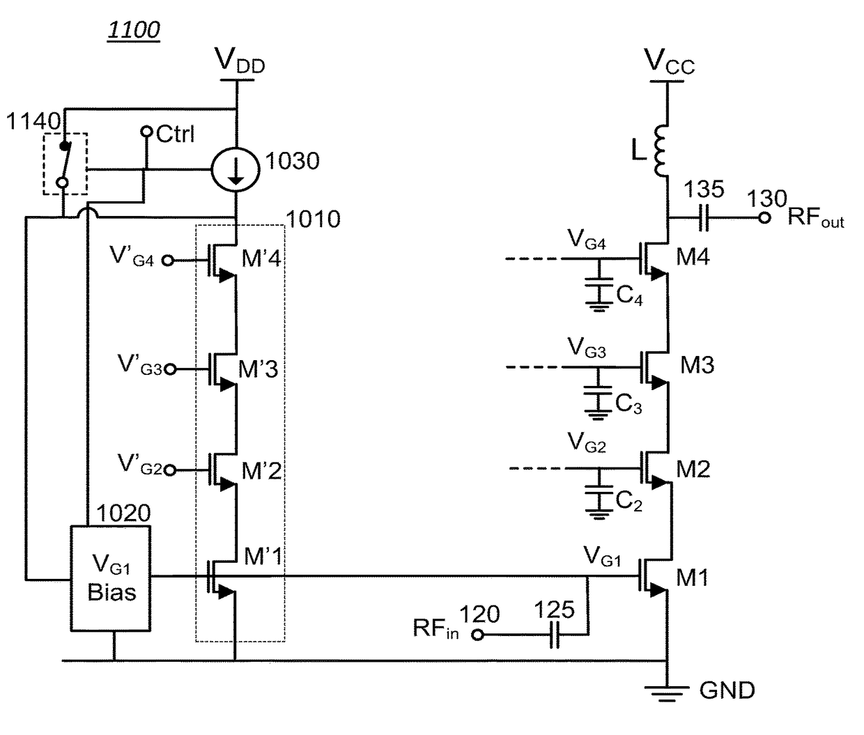
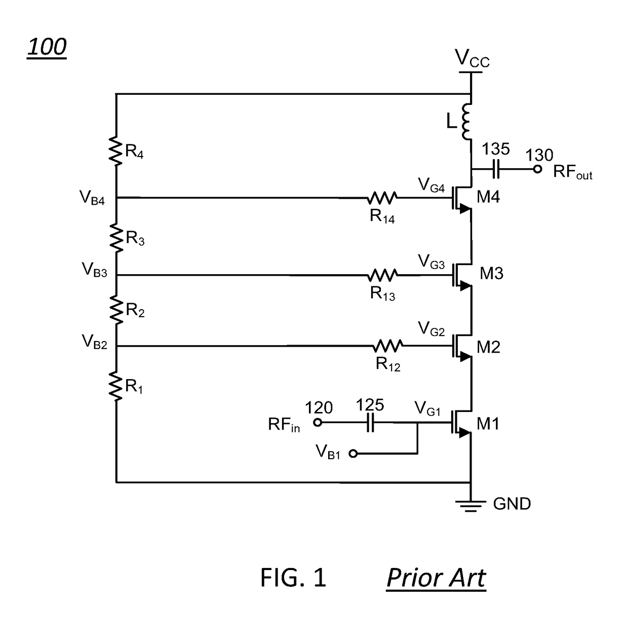
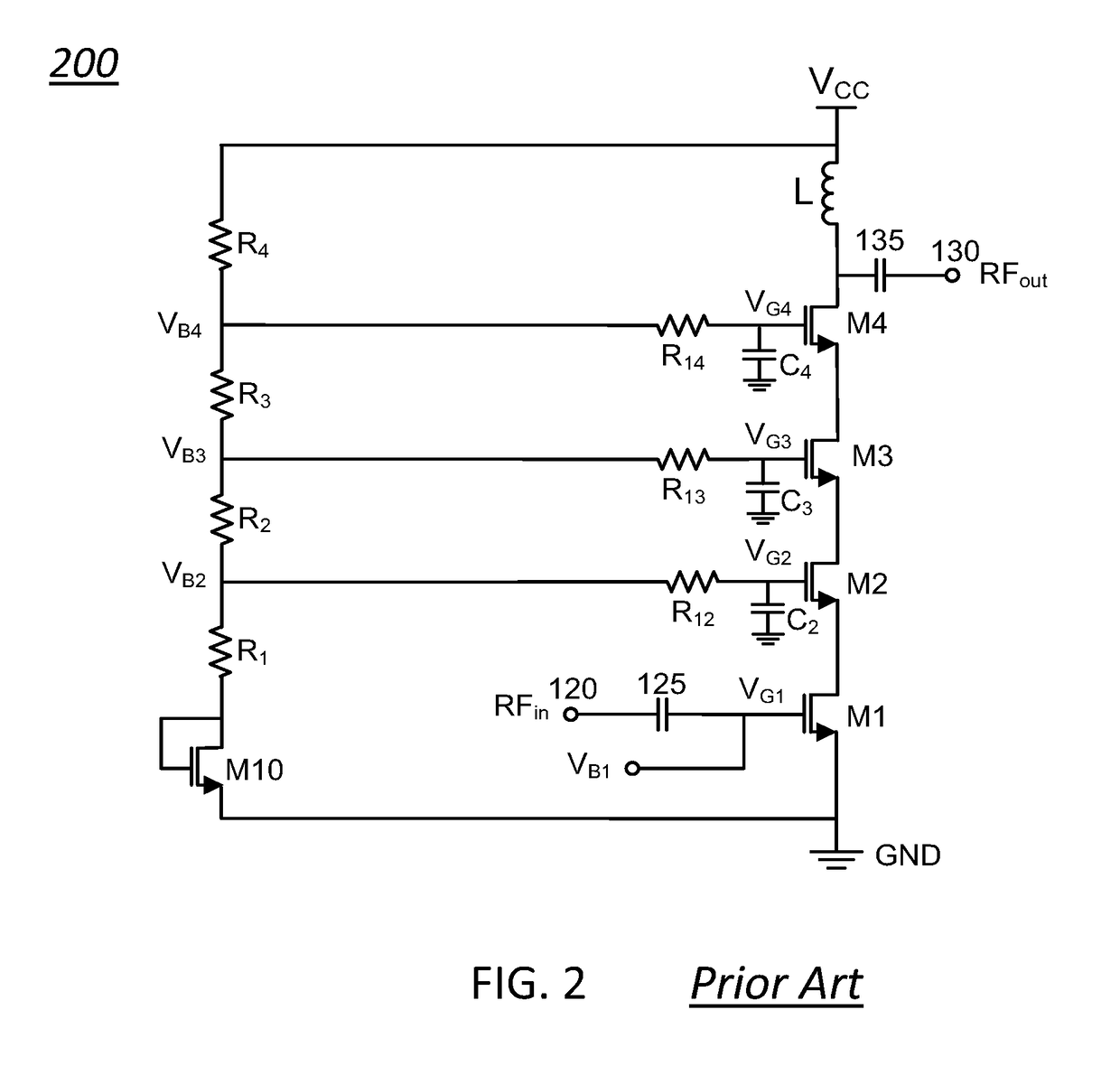
[0030]FIG. 1 shows a simplified schematic of a prior art stacked cascode (RF) amplifier (100). By way of example and not of limitation, the stacked cascode amplifier (100) can comprise a stack of FET transistors (M1, M2, M3, M4) that include an input transistor M1, cascode transistors (M4, M3, M2), and an output transistor M4. An input RF signal, RFin, provided at an input terminal (120) of the amplifier (100) is routed to a gate of the input transistor, M1, and is amplified by the amplifier (100). A corresponding amplified output RF signal, RFout, is provided at a drain of the output transistor, M4, and routed to an output terminal (13...


PUM


Abstract

Various methods and circuital arrangements for biasing one or more gates of stacked transistors of an amplifier are possible where the amplifier is configured to operate in at least an active mode and a standby mode. Circuital arrangements can reduce bias circuit standby current during operation in the standby mode while allowing a quick recovery to normal operating conditions of the amplifier. Biasing an input transistor of the stacked transistors can be obtained by using a replica stack circuit.

Description

CROSS REFERENCE TO RELATED APPLICATIONS[0001]The present application is related to U.S. application Ser. No. 15 / 268,275 entitled “Gate Drivers for Stacked Transistors Amplifiers” filed on Sep. 16, 2016, the disclosure of which is incorporated herein by reference in its entirety. The present application is also related to U.S. application Ser. No. 15 / 268,229 entitled “Cascode Amplifier Bias Circuits” filed on Sep. 16, 2016, the disclosure of which is incorporated herein by reference in its entirety. The present application is also related to U.S. application Ser. No. 15 / 268,257 entitled “Body Tie Optimization for Stacked Transistor Amplifier” filed on Sep. 16, 2016, the disclosure of which is incorporated herein by reference in its entirety.[0002]The present application may be related to U.S. Pat. No. 7,248,120, issued on Jul. 24, 2007, entitled “Stacked Transistor Method and Apparatus”, the disclosure of which is incorporated herein by reference in its entirety. The present applicat...

Claims


Application Information

Patent Timeline
Patent Type & Authority Patents(United States)
IPC IPC(8): H03F1/02H03F3/193H03F1/56
CPCH03F1/0227H03F1/56H03F3/193H03F2200/18H03F2200/453H03F2200/249H03F1/223H03F1/301H03F3/189
Inventor WAGH, POOJANPAL, KASHISH
Owner PSEMI CORP
Why Eureka
Try Eureka