Power supply circuit and semiconductor memory device including the same

a power supply circuit and semiconductor technology, applied in the field of electronic devices, can solve the problems that volatile memory devices cannot maintain data without, and achieve the effects of less chip area, increased output voltage range, and decreased voltage drop

Active Publication Date: 2018-01-02
SK HYNIX INC
View PDF8 Cites 0 Cited by
  • Summary
  • Abstract
  • Description
  • Claims
  • Application Information

AI Technical Summary

Benefits of technology

[0025]According to the exemplary embodiments of the present invention, it is possible to provide a power supply circuit that occupies less chip area, has a decreased voltage drop, and an increased output voltage range, and a semiconductor memory device including the same.

Problems solved by technology

Volatile memory devices are unable to maintain their data without a constant source of power.

Method used


Image

  • Power supply circuit and semiconductor memory device including the same
  • Power supply circuit and semiconductor memory device including the same
  • Power supply circuit and semiconductor memory device including the same

Examples


Embodiment Construction

[0031]Hereinafter, exemplary embodiments of the present invention will be described in detail with reference to the accompanying drawings. Like reference numerals refer to like elements throughout the specification. In the following description, when the detailed description of well-known functions or configurations is unnecessary to those skilled in the art to practice this invention, it is not provided. Further, names of constituent elements used may be selected for simplicity and may be different from names of components of an actual product.

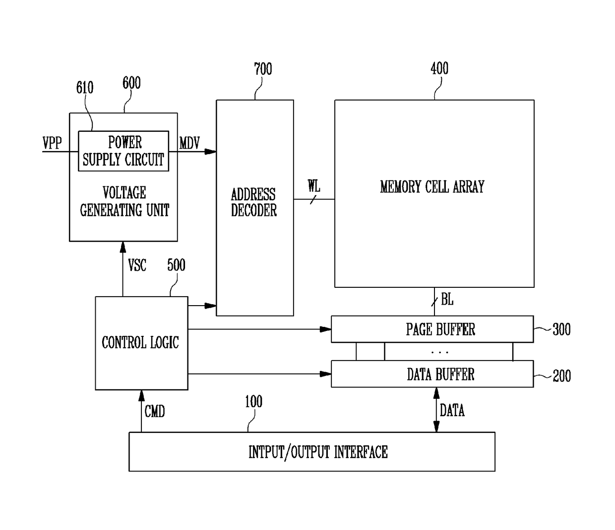
[0032]FIG. 1 is a diagram for describing a semiconductor memory device according to an exemplary embodiment of the present invention. Referring to FIG. 1, a semiconductor memory device may include an input / output interface 100, a data buffer 200, a page buffer 300, a memory cell array 400, a control logic 500, a voltage generating unit 600, and an address decoder 700.

[0033]The input / output interface 100 may receive data DATA and a command CMD...


PUM


Abstract

A power supply circuit includes a first transistor and a second transistor electrically coupled between a power supply terminal and an output terminal. When a first current path, in which output terminal through the first transistor, is formed, a voltage level of the output terminal may be controlled to be greater than or equal to a predetermined level. When a second current path, in which a current flows from the power supply terminal to the output terminal through the second transistor, is formed, the voltage level of the output terminal may be controlled to be less than or equal to the predetermined level.

Description

CROSS-REFERENCE TO RELATED APPLICATION[0001]The present application claims priority to Korean patent application number 10-2015-0029824 filed on Mar. 3, 2015, in the Korean Intellectual Property Office, the entire disclosure of which is incorporated by reference herein.BACKGROUND[0002]1. Field[0003]The present invention relates to an electronic device, and more particularly, to a power supply circuit and a semiconductor memory device including the same.[0004]2. Discussion of Related Art[0005]Instead of Hard Disk Drives (HDD), which are slow, heavy, large, and emit noise, the use of semiconductor memory devices has increased.[0006]Semiconductor memory devices are memory devices that use semiconductors, such as silicon (Si), germanium (Ge), gallium arsenide (GaAs), and indium phosphide (InP). Semiconductor memory devices are generally classified into volatile and nonvolatile memory devices.[0007]Volatile memory devices are unable to maintain their data without a constant source of pow...

Claims


Application Information

Patent Timeline
Patent Type & Authority Patents(United States)
IPC IPC(8): G11C11/34G11C5/14G11C7/10
CPCG11C5/147G11C7/1084
Inventor KOO, BON KWANG
Owner SK HYNIX INC
Why Eureka
Try Eureka