
Optical modulation device including liquid crystals, driving method thereof, and optical display device using the same

a technology of optical display device and liquid crystal, which is applied in the direction of optics, instruments, diffraction gratings, etc., can solve the problem of 3d texture generation, achieve the effect of improving the phase modulation characteristic of light, improving the display quality of optical display device, and being easy to control

Active Publication Date: 2018-01-09
SAMSUNG DISPLAY CO LTD
View PDF14 Cites 0 Cited by
  • Summary
  • Abstract
  • Description
  • Claims
  • Application Information

AI Technical Summary

Benefits of technology

The present patent describes an optical modulation device that can improve the display quality of 3D optical display devices by controlling the liquid crystal molecules and reducing texture. This is achieved through a two-step driving method that ensures reproducibility in the phase modulation characteristic of the device, resulting in improved display quality.

Problems solved by technology

However, in a region where there are strong horizontal and vertical fields due to large voltage differences, texture may be generated in 3D mode since alignment of the liquid crystal molecules is unstable.

Method used


Image

  • Optical modulation device including liquid crystals, driving method thereof, and optical display device using the same
  • Optical modulation device including liquid crystals, driving method thereof, and optical display device using the same
  • Optical modulation device including liquid crystals, driving method thereof, and optical display device using the same

Examples


Embodiment Construction

[0049]Embodiments of the present disclosure will be described more fully hereinafter with reference to the accompanying drawings, in which exemplary embodiments of the disclosure are shown.

[0050]As those skilled in the art would realize, the described embodiments may be modified in various different ways, all without departing from the spirit or scope of the present disclosure.

[0051]In the drawings, the thickness of layers, films, panels, regions, etc. may be exaggerated for clarity.

[0052]Like reference numerals may designate like elements throughout the specification.

[0053]It will be understood that when an element such as a layer, film, region, or substrate is referred to as being “on” another element, it can be directly on the other element or intervening elements may also be present.

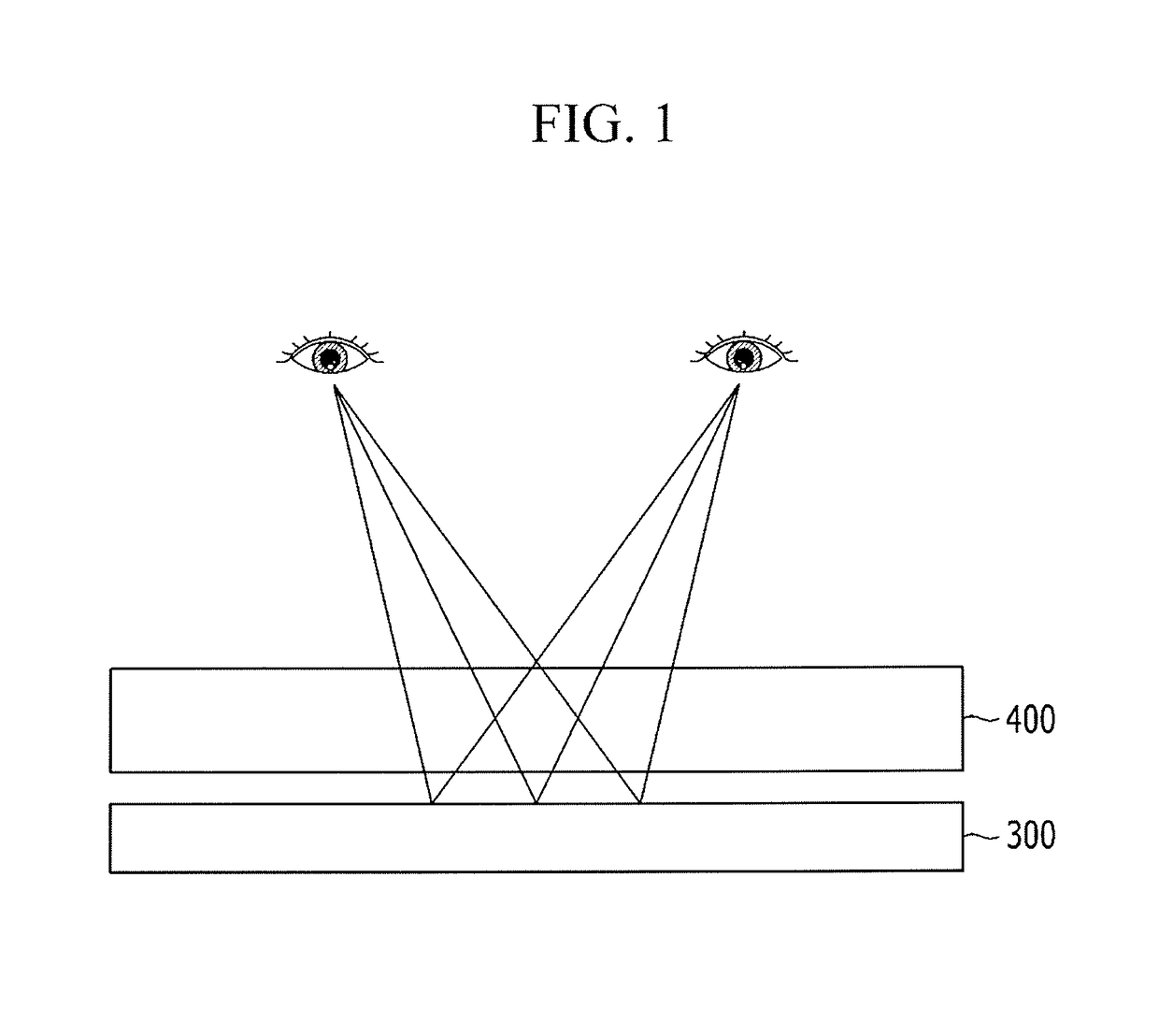
[0054]FIG. 1 illustrates a schematic structure of an optical display device according to an exemplary embodiment of the present disclosure and a method of generating a 2D image.

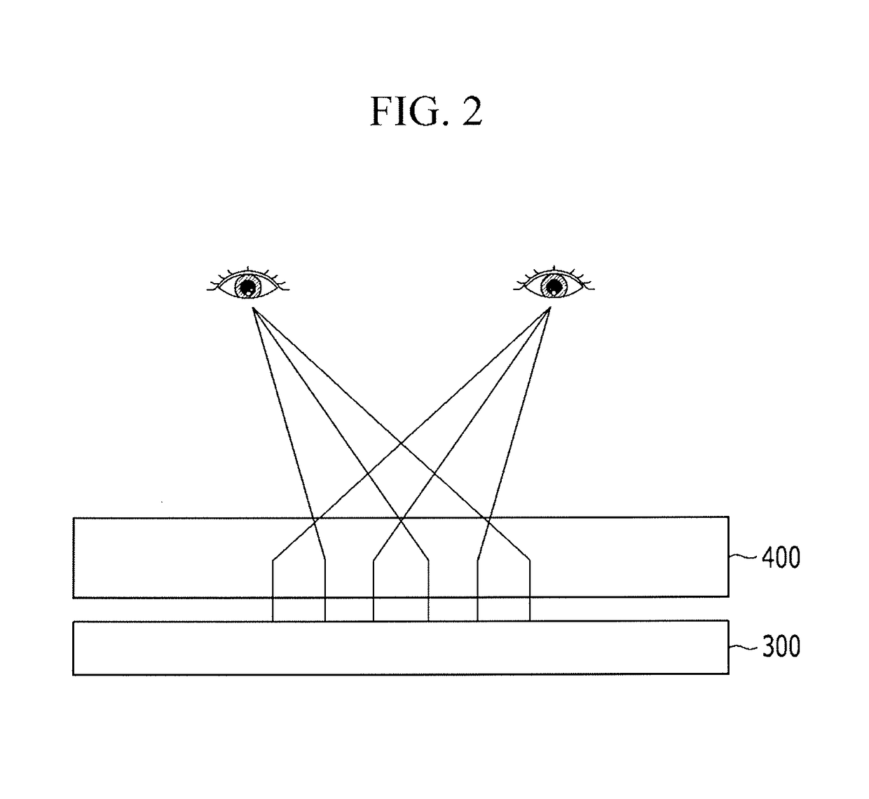
[0055]FIG. 2 illustrat...


PUM

PropertyMeasurementUnit
timeaaaaaaaaaa
time t1aaaaaaaaaa
common voltageaaaaaaaaaa

Abstract

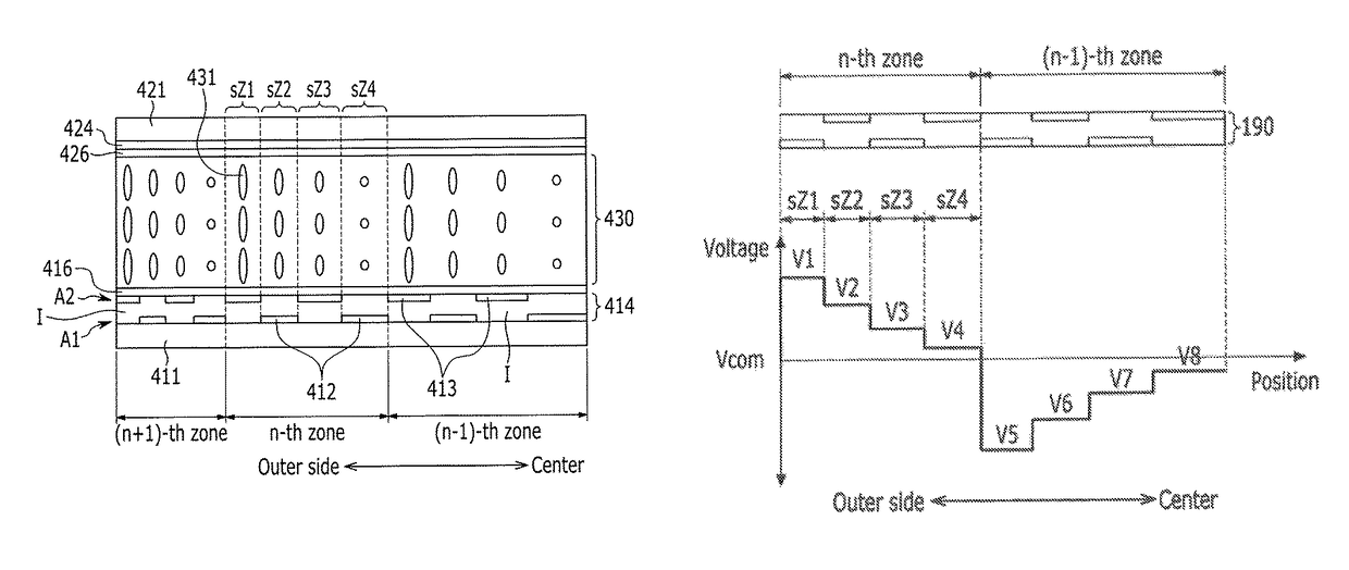
An optical modulation device includes a first electrode layer in which a plurality of electrodes are arranged and a second electrode layer, where the optical modulation device configures a Fresnel zone plate wherein groups of adjacent electrodes of the plurality of electrodes define zones of the Fresnel zone plate. A method of driving the optical modulation device includes applying a common voltage to the second electrode layer, applying starting voltages to the first electrode layer in a first step, applying lens voltages to the first electrode layer in a second step, where polarities of the lens voltages with respect to the common voltage are inverted for every zone, and an absolute difference between starting voltages applied to electrodes adjacent to a zone boundary in the first step is less than an absolute difference of the lens voltages applied to electrodes adjacent to a zone boundary in the second step.

Description

CROSS-REFERENCE TO RELATED APPLICATION[0001]This application claims priority under 35 U.S.C. §119 from Korean Patent Application No. 10-2015-0004404 filed in the Korean Intellectual Property Office on Jan. 12, 2015, and all the benefits accruing therefrom, the contents of which are herein incorporated by reference in their entirety.BACKGROUND[0002](a) Technical Field[0003]Embodiments of the present disclosure are directed to an optical modulation device, a driving method thereof, and an optical display device using the same, and more particularly, to an optical modulation device including liquid crystals, a driving method thereof, and an optical display device using the same.[0004](b) Discussion of the Related Art[0005]Optical display devices that use an optical modulation device for modulating characteristics of light have been recently developed.[0006]For example, for a 3-dimensional (3D) optical display device, an optical modulation device is used to divide an image into differen...

Claims


Application Information

Patent Timeline
Patent Type & Authority Patents(United States)
IPC IPC(8): G02F1/137G02F1/29G02B27/26G02B5/18G02B27/22G02F1/1343G02B30/25G02B30/28G02B30/29
CPCG02B27/26G02B5/1876G02B5/1885G02F1/29G02B27/2214G02F2203/28G02F1/134309G02B30/28G02B30/29H04N13/30G02B26/06G02B30/34G02B30/25G02B30/27
Inventor YI, JUNG HWANJUNG, KYUNG HO
Owner SAMSUNG DISPLAY CO LTD
Learn More