RF impedance matching network

a technology of impedance matching and impedance matching, applied in electrical discharge tubes, semiconductor/solid-state device testing/measurement, electrical equipment, etc., can solve problems such as mechanical failure, failure of vvc replacement, and downtime of fabrication equipment, so as to reduce the time it takes

Active Publication Date: 2018-01-09
ASM AMERICA INC
View PDF187 Cites 35 Cited by
  • Summary
  • Abstract
  • Description
  • Claims
  • Application Information

AI Technical Summary

Benefits of technology

[0014]The present invention is directed toward an RF impedance matching network which utilizes electronically variable capacitors (EVCs) to reduce the time it takes to create an impedance match. Such an RF impedance matching network is advantageously employed in semiconductor fabrication systems and processes.

Problems solved by technology

In complex semiconductor fabrication processes using plasma chambers, where the impedance changes are often frequent, the frequent adjustments needing to be made to a VVC leads to mechanical failures, often within less than a year of use for individual VVCs.
Failure of a VVC leads to downtime for fabrication equipment so that the failed VVC can be replaced.
As semiconductor devices shrink in size and become more complex, the feature geometries become very small.
During a significant amount of the matching process, which includes the microprocessor determining the capacitances for the VVCs needed to create the match, controlling the VVCs to the achieve the determined capacitances, and then finally time for the RF matching network circuits to stabilize with the new capacitances, the fabrication process parameters are unstable, and these unstable process parameters must be accounted for as part of the overall fabrication process.
Because the matching process time is becoming a more and more significant part of the time for each fabrication process step, the period in which process parameters are unstable becomes more of a factor in the overall fabrication process.
However, because an EVC is purely an electronic device, an EVC is not a one-for-one replacement for a VVC in an RF matching network.
These approaches, however, are time consuming in an industry where speed is of increasing value.

Method used


Image

  • RF impedance matching network
  • RF impedance matching network
  • RF impedance matching network

Examples


Embodiment Construction

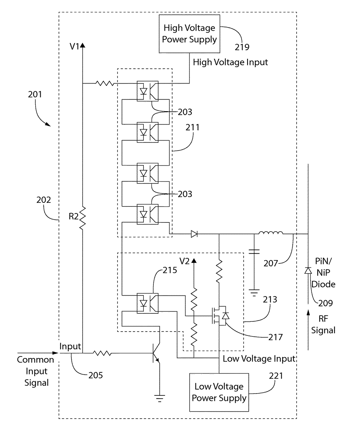
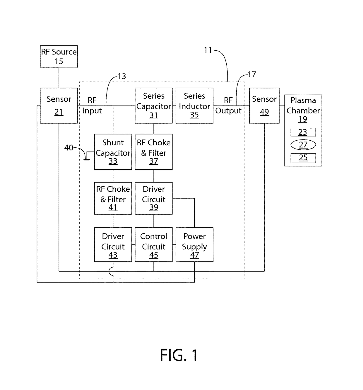
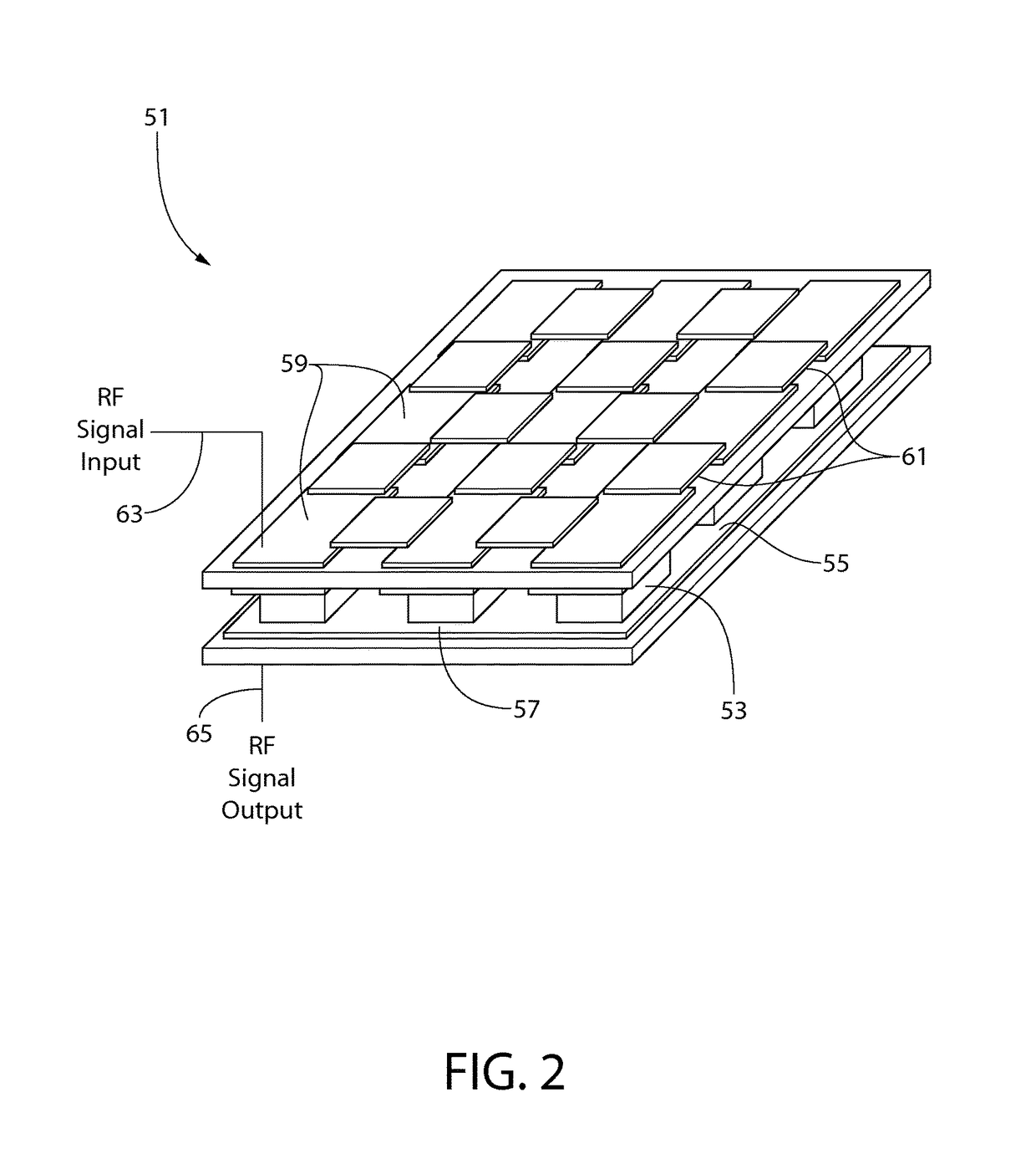
[0031]The description of illustrative embodiments according to principles of the present invention is intended to be read in connection with the accompanying drawings, which are to be considered part of the entire written description. In the description of embodiments of the invention disclosed herein, where circuits are shown and described, one of skill in the art will recognize that for the sake of clarity, not all desirable or useful peripheral circuits and / or components are shown in the figures or described in the description. Moreover, the features and benefits of the invention are illustrated by reference to the disclosed embodiments. Accordingly, the invention expressly should not be limited to such disclosed embodiments illustrating some possible non-limiting combinations of features that may exist alone or in other combinations of features; the scope of the invention being defined by the claims appended hereto.

[0032]As used throughout, ranges are used as shorthand for descr...


PUM


Abstract

An RF impedance matching network includes an RF input configured to operably couple to an RF source, the RF source having a fixed RF source impedance; an RF output configured to operably couple to a plasma chamber, the plasma chamber having a variable plasma impedance; a series EVC; a shunt EVC; an RF input sensor; and a control circuit configured to: determine an input impedance; determine the plasma impedance; determine a first capacitance value for the series variable capacitance and a second capacitance value for the shunt variable capacitance, the determination of the first capacitance value and the second capacitance value based on the plasma impedance and the RF source impedance; generate a control signal to alter at least one of the series variable capacitance and the shunt variable capacitance to the first capacitance value and the second capacitance value, respectively.

Description

CROSS REFERENCE TO RELATED APPLICATIONS[0001]The present application is a continuation in part of U.S. patent application Ser. No. 14 / 594,262, filed Jan. 12, 2015, which in turn claims priority to U.S. Provisional Patent Application Ser. No. 61 / 925,974, filed Jan. 10, 2014. The present application also claims priority to U.S. Provisional Patent Application Ser. No. 61 / 940,139, filed Feb. 14, 2014. The disclosures of these references are incorporated herein by reference in their entireties.FIELD OF THE INVENTION[0002]The field of the present invention relates to RF impedance matching networks, and particularly to RF impedance matching networks that may be used with plasma chambers used in the fabrication of semiconductor devices.BACKGROUND OF THE INVENTION[0003]The semiconductor device fabrication process uses plasma processing at different stages to make semiconductor devices, which may include a microprocessor, a memory chip, and other types integrated circuits and devices. Plasma ...

Claims


Application Information

Patent Timeline
Patent Type & Authority Patents(United States)
IPC IPC(8): H01L21/302H01L21/3213H01L21/311H01L21/3065H01L21/02H01L21/285H01L21/66H01J37/32H01L21/67
CPCH01J37/32183H01L22/10H01L21/67069H01L21/02252H01L21/02263H01L21/0262H01L21/3065H01L21/31116H01L21/31138H01L21/32136H01L21/28506H01L22/26H01J37/32082H03H7/40
Inventor BHUTTA, IMRAN AHMED
Owner ASM AMERICA INC
Why Eureka
Try Eureka