

Separation method of GaN substrate by wet etching
a technology of wet etching and gan, which is applied in the direction of basic electric elements, electrical equipment, semiconductor devices, etc., can solve the problems of high brightness in high output operation, increase in fabrication costs, and complicated fabrication process, so as to improve the epitaxial growth of gan, reduce fabrication costs, and simple process
- Summary
- Abstract
- Description
- Claims
- Application Information
AI Technical Summary
Benefits of technology
Problems solved by technology
Method used
Image

Examples
Embodiment Construction
[0019]Embodiments of the invention will now be described in detail with reference to the accompanying drawings. It should be understood that the following embodiments are given by way of illustration only and the present invention is not limited to the following embodiments. Rather, it should be understood that various modifications, variations and alterations can be made without departing from the spirit and scope of the present invention defined by the claims and equivalents thereof.
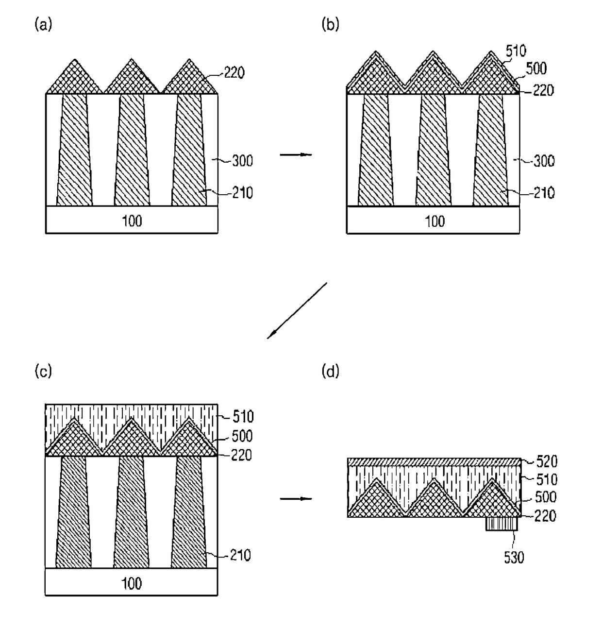
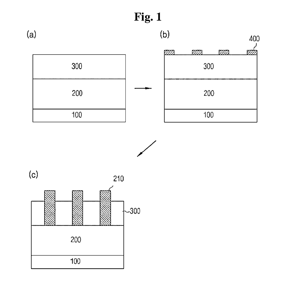
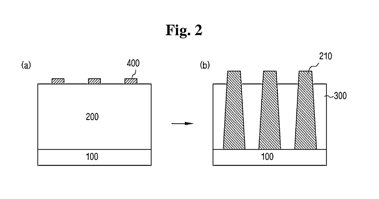
[0020]The present invention relates to a method of separating a GaN substrate using a chemical lift-off process. The method includes: forming oxide layers separated from each other and a GaN column in each space between the oxide layers on a substrate; forming an n-GaN layer covering an upper space above the oxide layers and the n-GaN columns; sequentially forming an active layer, a p-GaN layer, and a p-type electrode on the n-GaN layer; and removing the oxide layers and wet etching the n-GaN columns t...
PUM
| Property | Measurement | Unit |
|---|---|---|
| thickness | aaaaa | aaaaa |
| thick | aaaaa | aaaaa |
| concentration | aaaaa | aaaaa |
Abstract
Description
Claims
Application Information