Optical waveguide device and method of manufacturing the same

a technology of optical waveguides and applied in the direction of optical waveguide light guides, instruments, optics, etc., can solve the problems of increased optical loss, impaired high-speed operation, and difficulty in high-speed refractive index modulation with low optical loss, and achieve low driving voltage, small quality variation, and low optical loss

Active Publication Date: 2018-01-30
ADVANCED MICRO FOUNDRY PTE LTD
View PDF9 Cites 2 Cited by
  • Summary
  • Abstract
  • Description
  • Claims
  • Application Information

AI Technical Summary

Benefits of technology

[0023]According to the optical waveguide device according to the above-described aspect, it is possible to realize an optical waveguide device that is suitable for a small-footprint optical integrated circuit such as an optical modulator enabling high-speed refractive index modulation with low optical loss and low driving voltage and allows only small quality variation for applications to optical fiber communication devices, in particular, optical transport equipment used for long-haul or metro-area wavelength-division multiplexing optical-fiber communication and optical-interconnect equipment used in data centers and the like.

Problems solved by technology

However, in this case, there is a problem of an increase in optical loss due to an increase of optical absorption by carriers.
In addition, there is another problem that it is not possible to reduce parasitic capacitance caused by the fringe electric fields from slab regions existing in side sections of the rib waveguide and high-speed operation is impaired.
Therefore, in a case in which the above-described silicon rib waveguide is used, high-speed refractive index modulation with low optical loss is difficult.
In a design based on NPL 1, when a rib waveguide having a corrugated distribution profile in high refractive index contrast is used, return loss is decreased due to Bragg reflection and optical feedback to a laser light source generating incident light to the optical modulator is significant and mode hopping is generated, whereby the laser light source becomes unstable.
As a result, there is a problem that it is not possible to generate stabilized optical modulation signals.
Therefore, there is a problem that it is not possible to reduce the driving voltage.
Furthermore, in PTL 2, there are additional problems that the influence of fabrication error is significant and it is not possible to provide an optical modulator with small quality variation.

Method used


Image

  • Optical waveguide device and method of manufacturing the same
  • Optical waveguide device and method of manufacturing the same
  • Optical waveguide device and method of manufacturing the same

Examples


example 1

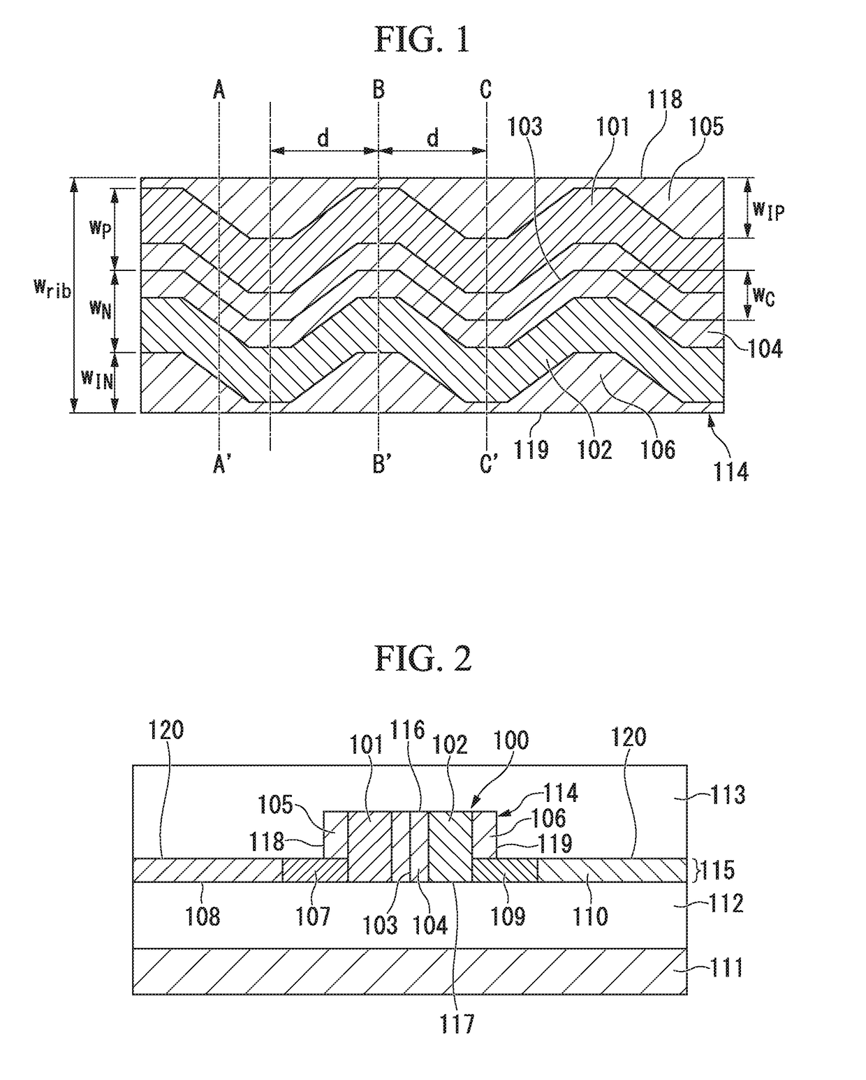
[0080]The fabrication method and configuration of an optical waveguide device that functions based on the above-described configuration and principle will be described in detail using the cross-sectional configuration of FIG. 2 as an example. A rib waveguide 200 illustrated in FIG. 8 is fabricated on a silicon-on-insulator (SOI) layer using an SOI wafer through photolithography and etching. The substrate in an SOI wafer serves as a substrate 211, and a buried oxidized layer in the SOI wafer serves as a lower cladding 212. The thickness of the lower cladding 212 in the vertical direction is 2 μm.

[0081]An optical resist is applied onto the rib waveguide 200, and an optical resist 221 having a cross-sectional shape illustrated in FIG. 9 is obtained through photolithography. A top surface 216 and side walls 218 and 219 on both sides of a rib 214 in the center of the rib waveguide 200, the entire area of a top surface 220A of a slab 215 on the left side of the rib 214 in the width direct...

example 2

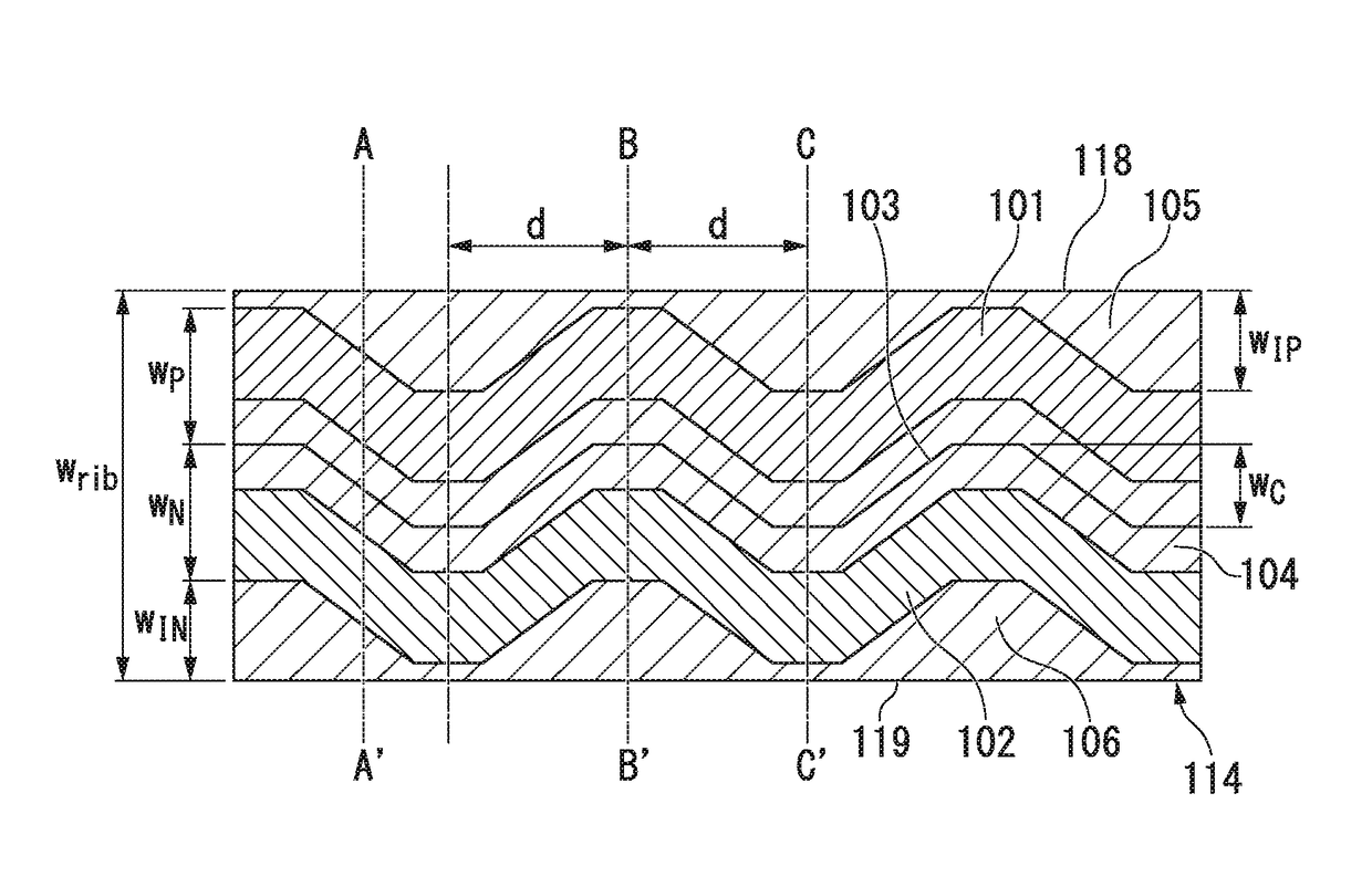
[0091]In the present example, a second configuration of the optical waveguide device of the invention will be described. FIG. 14 schematically illustrates a top view illustrating a rib in the example. A cross-sectional view of an optical waveguide device including the rib waveguide is schematically illustrated in FIG. 15. Since the constituents of a substrate 311, a lower cladding 312, an upper cladding 313, a rib 314 and a slab 315 in a rib waveguide 300 are same as those of the substrate 111, the lower cladding 112, the upper cladding 113, the rib 114 and the slab 115 in the rib waveguide 100 in Example 1 respectively, they will not be described again here.

[0092]A P-doped P region 301 and an N-doped N region 302 are distributed in corrugated shapes in the propagating direction of the guided light. The width wN2 of the N region 302 is substantially constant in the propagating direction of guided light, and wN2=wN (refer to FIG. 1). For example, when wrib2 is 500 nm, wN2 is 90 nm. O...

example 3

[0101]A configuration of an optical waveguide device functioning as a Mach-Zehnder (MZ) optical modulator will be described using the optical waveguide device described in Example 1 or 2. A block diagram of the configuration of the MZ optical modulator is illustrated in FIG. 19. The MZ optical modulator consists of the following components:

input waveguide 1905;

1×2 splitter section 1903;

first arm consisting of a waveguide 1906, a phase shifter 1901 and a waveguide 1908; second arm consisting of a waveguide 1907, a phase shifter 1902 and a waveguide 1909;

2×1 coupler section 1904; and

output waveguide 1910.

[0102]An input port of the 1×2 splitter section 1903 is connected to the input waveguide 1905, and two output ports of the 1×2 splitter section 1903 are respectively connected to the two arms. Two input ports of the 2×1 coupler section 1904 are respectively connected to the two arms, and an output port of the 2×1 coupler section 1904 are connected to the output waveguide 1910.

[0103]Th...


PUM

PropertyMeasurementUnit
refractive indexaaaaaaaaaa
width wribaaaaaaaaaa

Abstract

An optical waveguide device includes a substrate; a lower cladding disposed on the substrate; a rib waveguide including a slab disposed on the lower cladding and a single rib disposed on the slab contiguous to the slab; and an upper cladding disposed on the rib waveguide. The rib waveguide includes a first doped region having a first electric conductivity exhibiting a P-type electric conductivity across the rib and the slab and a second doped region being contiguous to the first doped region and having a second electric conductivity exhibiting an N-type electric conductivity across the rib and the slab.

Description

CROSS REFERENCE TO RELATED APPLICATIONS[0001]This application is a continuation application based on a PCT Patent Application No. PCT / JP2014 / 060558, filed Apr. 7, 2014.BACKGROUND OF THE INVENTION[0002]Field of the Invention[0003]The present invention relates to an optical waveguide device that enables high-speed refractive index modulation with low optical loss and low driving voltage and a method of manufacturing the optical waveguide device.[0004]Description of the Related Art[0005]In recent years, the application of small-footprint optical integrated circuits such as planar optical waveguides to optical-fiber communication devices, in particularly, to optical transport equipment used for long-haul or metro-area wavelength-division multiplexing optical-fiber communication and optical interconnect equipment used in data centers and the like has been studied.[0006]U.S. Pat. No. 7,085,443 (hereinafter referred to as PTL 1) discloses a single-mode silicon rib waveguide, in which refra...

Claims


Application Information

Patent Timeline
Patent Type & Authority Patents(United States)
IPC IPC(8): G02F1/025G02F1/015G02F1/21G02B6/12G02F1/00
CPCG02F1/025G02F1/015G02F2001/212G02F1/0018G02F2001/0151G02B2006/12097G02F1/0151G02F1/212
Inventor OGAWA, KENSUKEGOI, KAZUHIROLO, GUO-QIANGLIOW, TSUNG-YANG JASONTU, XIAOGUANG
Owner ADVANCED MICRO FOUNDRY PTE LTD
Why Eureka
Try Eureka