Photoelectric conversion device

a conversion device and photoelectric technology, applied in the field of photoelectric transducers, can solve the problems of reducing photoelectric conversion efficiency, two problems cannot be solved simultaneously, and conductor loss, so as to improve mobility, reduce conductor loss, and efficiently enter the charge-separating means

Inactive Publication Date: 2005-08-04
SONY CORP
View PDF9 Cites 79 Cited by
  • Summary
  • Abstract
  • Description
  • Claims
  • Application Information

AI Technical Summary

Benefits of technology

[0022] According to the present invention, by providing the low-resistance region, i.e., high-conductivity region in the second electrode that is in contact with the charge-separating means, electrons generated by photoelectric conversion in the charge-separating means are collected in the low-resistance region. Since the collected electrons move into an external circuit through the low-resistance region, the above-described conductor loss is reduced. In this way, a low-loss path for the transfer of electrons (improvement of mobility) can be ensured.
[0023] Since the incident light is led to the transparent portion provided in the low-resistance region by the light-guiding means and then is led to the charge-separating means, the path of the incident light can be controlled such that at least the major portion of the incident light is incident on the charge-separating means. The loss of incident light, i.e., the loss of light energy caused by the reflection of the incident light from a region other than the transparent portion can be blocked; therefore, the incident light can efficiently enter the charge-separating means. Even when a light-absorbing layer such as a transparent conductive layer is present in the second electrode, the light-guiding means reduces the amount of light that is incident on the light absorbing layer, thus reducing the amount of light absorption. Since such a path of incident light can be achieved even when the transparent portion is reduced in width, the area of the low-resistance region can be enlarged to such a degree that the low-resistance region does not interfere with the path of incident light. As a result, generated electrons readily flow into the low-resistance region, and the conductivity of the electrode is increased. Consequently, both the conductor loss and the loss of light energy can be further suppressed.
[0024] The relatively simple structure formed only by providing the light-guiding means in addition to the first electrode, the second electrode, and the charge-separating means can reduce the conductor loss and the loss of light energy.

Problems solved by technology

However, both photoelectric transducers shown in FIGS. 10 and 11 mainly have the following two problems: Since the transparent conductive layer 55 has a relatively-high electrical resistance, when electrons pass through this layer, conductor loss (loss due to Joule heat generated by the electrical resistance of the conductor) occurs to reduce photoelectric conversion efficiency.
Since there is a trade-off between the two problems, the two problems cannot be simultaneously solved.
However, a decrease in the width and / or the cross-sectional area of the metal lines 57 increases the electrical resistance and reduces the conductive performance of the transparent conductive layer 55.
Since there is a trade-off between these problems, these problems cannot be simultaneously solved.
Furthermore, this complicated structure increases the manufacturing costs.

Method used


Image

  • Photoelectric conversion device
  • Photoelectric conversion device
  • Photoelectric conversion device

Examples


first embodiment

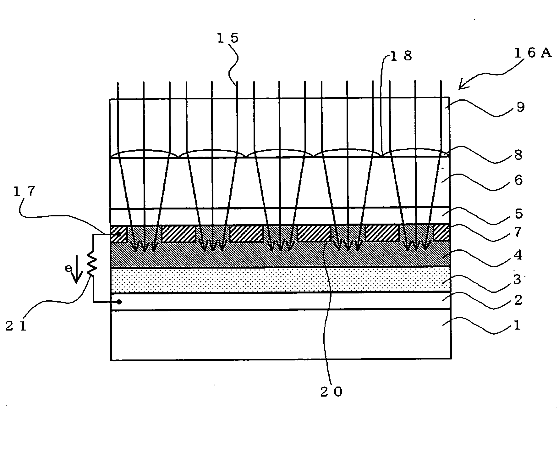
[0048] As shown in FIG. 1, in a photoelectric transducer 16A functioning as a wet solar cell according to this embodiment, a conductive layer 2 that is composed of, for example, ITO, gold, or platinum is formed on a substrate 1 composed of glass or a plastic by, for example, vacuum deposition, sputtering, chemical vapor deposition (CVD), or a sol-gel method.

[0049] An electrolytic layer 3 provided on the conductive layer 2 is composed of, for example, an electrolytic solution containing an iodine-iodide electrolyte and a mixed solvent containing acetonitrile and ethylene carbonate. The electrolytic solution contains, for example, 0.6 mol / L of tetrapropylammonium iodide and 5×10² mol / L of iodine.

[0050] A charge separating layer 4 includes a semiconductor sublayer such as an ultrafine TiO2 particle sublayer adsorbing a ruthenium complex, i.e., RuL2(NCS)2 (where L: 4,4′-dicarboxy-2,2′-bipyridine) functioning as sensitizing dye. This ultrafine particle sublayer is composed of sintered ...

second embodiment

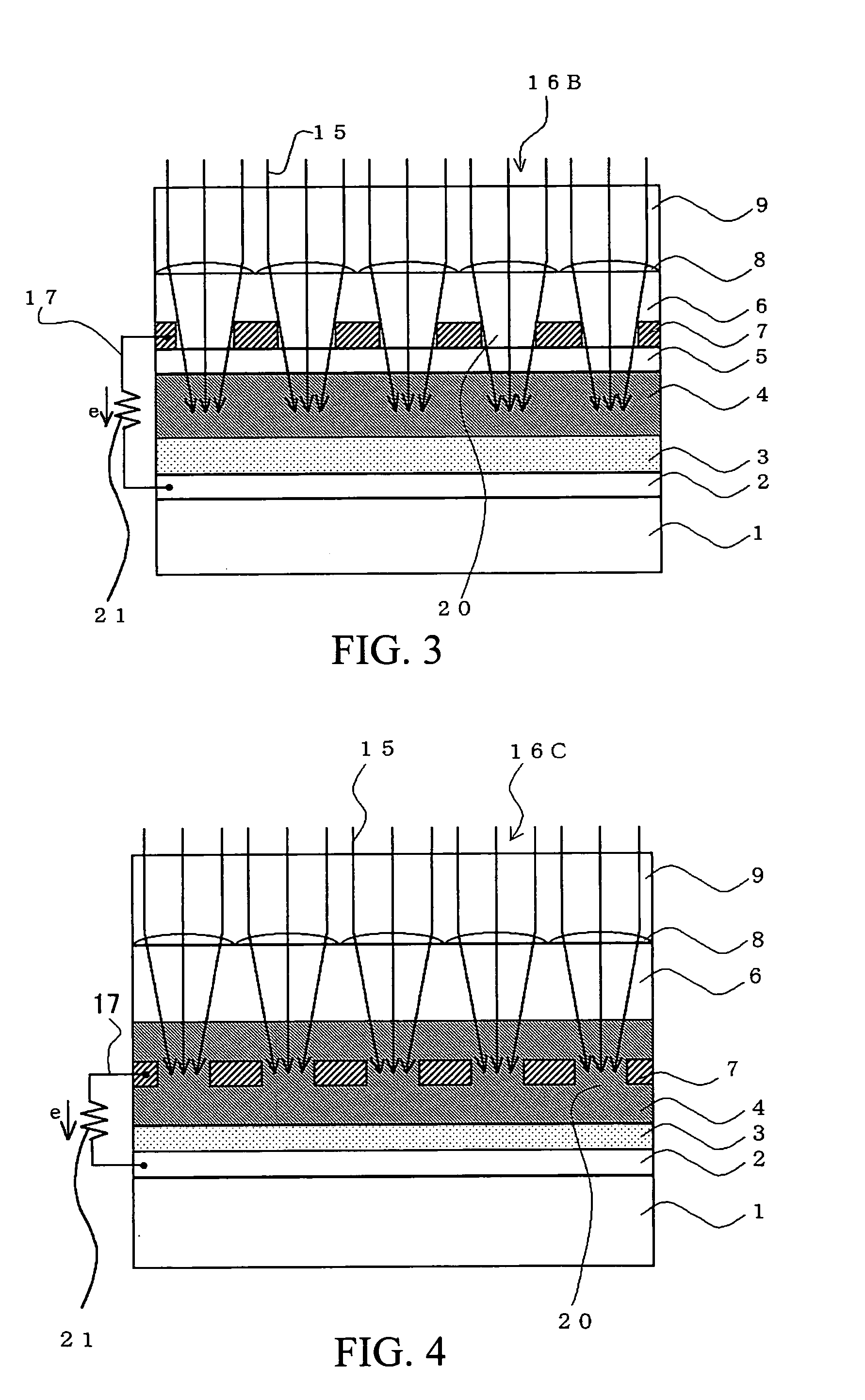
[0071] As shown in FIG. 3, the photoelectric transducer 16B of this embodiment is as in the first embodiment, but the metal lines 7 are provided not within the charge separating layer 4 but on the transparent conductive layer 5.

[0072] According to this embodiment, the incident light 15 converging on the openings 20 between the metal lines 7 passes through the transparent conductive layer 5 and then efficiently enters the charge separating layer 4. Hence, electrons generated in the charge separating layer 4 can readily pass through the transparent conductive layer 5 and flow into the metal lines 7.

[0073] This embodiment can also achieve the same effects as in the first embodiment described above.

third embodiment

[0074] As shown in FIG. 4, a photoelectric transducer 16C of this embodiment is as in the first embodiment, but the transparent conductive layer 5 is omitted and the metal lines 7 is disposed at the middle along the thickness direction in the charge separating layer 4.

[0075] In this embodiment, light energy is not absorbed in the transparent conductive layer 5 by virtue of the absence of the transparent conductive layer 5. Hence, almost all incident light 15 can enter the charge separating layer 4.

[0076] Since the metal lines 7 are disposed at the inside of the charge separating layer 4, electrons generated in the charge separating layer 4 directly flow into the metal lines 7; hence, the conductor loss caused by the passage of the electrons through the transparent conductive layer 5 does not occur. In case where incident light is partially reflected by the metal lines 7, only a minimal amount of light is reflected. Furthermore, since photocarriers are generated by the reflected li...


PUM

PropertyMeasurementUnit
diameteraaaaaaaaaa
thicknessaaaaaaaaaa
thicknessaaaaaaaaaa

Abstract

A photoelectric transducer having a relatively simple structure and capable of reducing the loss of light energy of incident light and conductor loss due to electrical resistance. A photoelectric transducer 16A includes a conductive layer 2; a electrolytic layer 3 that is in contact with the conductive layer 2; a charge separating layer 4; a transparent conductive layer 5 and a metal lines 7, which are in contact with the charge separating layer 4; and convex lenses 8 converging incident light 15 on openings 20 provided between the metal lines 7, the incident light 15 being converged on the charge separating layer 4 by the convex lenses 8. Electrons generated by photoelectric conversion move to the exterior through an external circuit 17 having a low resistivity.

Description

TECHNICAL FIELD [0001] The present invention relates to a photoelectric transducer suitable for a dye-sensitized photoelectric transducer such as a photoelectrochemical solar cell (hereinafter, referred to as “wet solar cell”). BACKGROUND ART [0002] Various dye-sensitized photoelectric transducers such as wet solar cells have been known. For example, FIG. 10 is a cross-sectional view showing an example of the basic structure of a photoelectric transducer 66A. [0003] This photoelectric transducer 66A includes the following constituents: A substrate 51 is composed of glass or a plastic, both of which have satisfactory mechanical strength. A conductive layer 52 composed of indium tin oxide (ITO) is provided on the substrate 51 by vapor deposition. An electrolytic layer 53 is provided on the conductive layer 52 and includes an electrolytic solution containing an iodine-iodide electrolyte and a mixed solvent containing acetonitrile and ethylene carbonate. [0004] A first charge separating...

Claims


Application Information

Patent Timeline
Patent Type & Authority Applications(United States)
IPC IPC(8): H01G9/20H01L31/04H01L27/146H01L31/0232H01L31/052H01L51/00H01L51/30H01L51/44H01M14/00
CPCH01G9/2031H01G9/2068H01G9/209H01L27/14627H01L31/0232H01L31/0543H01L51/447H01M14/005Y02E10/52Y02E10/542H01L51/0086H01L31/02325H10K85/344H10K30/87
Inventor IMOTO, TSUTOMUENOMOTO, MASASHI
Owner SONY CORP
Why Eureka
Try Eureka