Wavelength-converted semiconductor light emitting device

a light-emitting device and wavelength-converting technology, which is applied in the direction of solid-state devices, basic electric elements, electrical appliances, etc., can solve the problems of significant light attenuation, poor extraction efficiency, and inability to completely eliminate optical losses, etc., to achieve efficient extraction of light from the light-emitting region, high efficiency, and high absorbency

Active Publication Date: 2008-03-11
LUMILEDS
View PDF39 Cites 81 Cited by
  • Summary
  • Abstract
  • Description
  • Claims
  • Application Information

AI Technical Summary

Benefits of technology

[0007]In accordance with embodiments of the invention, a material such as a phosphor is optically coupled to a semiconductor structure including a light emitting region disposed between an n-type region and a p-type region, in order to efficiently extract light from the light emitting region into the phosphor. The phosphor may be phosphor grains in direct contact with a surface of the semiconductor structure, or a ceramic phosphor bonded to the semiconductor structure, or to a thin nucleation structure on which the semiconductor structure may be grown. The phosphor is preferably highly absorbent and highly efficient. When the semiconductor structure emits light into such a highly efficient, highly absorbent phosphor, the phosphor may efficiently extract light from the structure, reducing the optical losses present in prior art devices.

Problems solved by technology

The use of a sapphire substrate may lead to poor extraction efficiency due to the large difference in index of refraction at the interface between the semiconductor layers and the substrate.
These many passes result in significant attenuation of the light due to optical losses at contacts, free carrier absorption, and interband absorption within any of the III-nitride device layers.
The use of other growth substrates with an index of refraction that more closely matches that of the III-nitride material may reduce but generally will not completely eliminate the optical losses.
Similarly, due to the large difference in index of refraction between III-nitride materials and air, elimination of the growth substrate also will not eliminate the optical losses.

Method used


Image

  • Wavelength-converted semiconductor light emitting device
  • Wavelength-converted semiconductor light emitting device
  • Wavelength-converted semiconductor light emitting device

Examples


Embodiment Construction

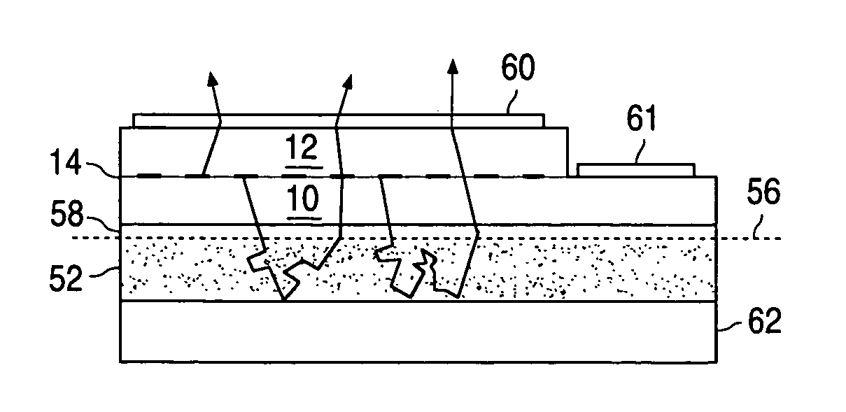
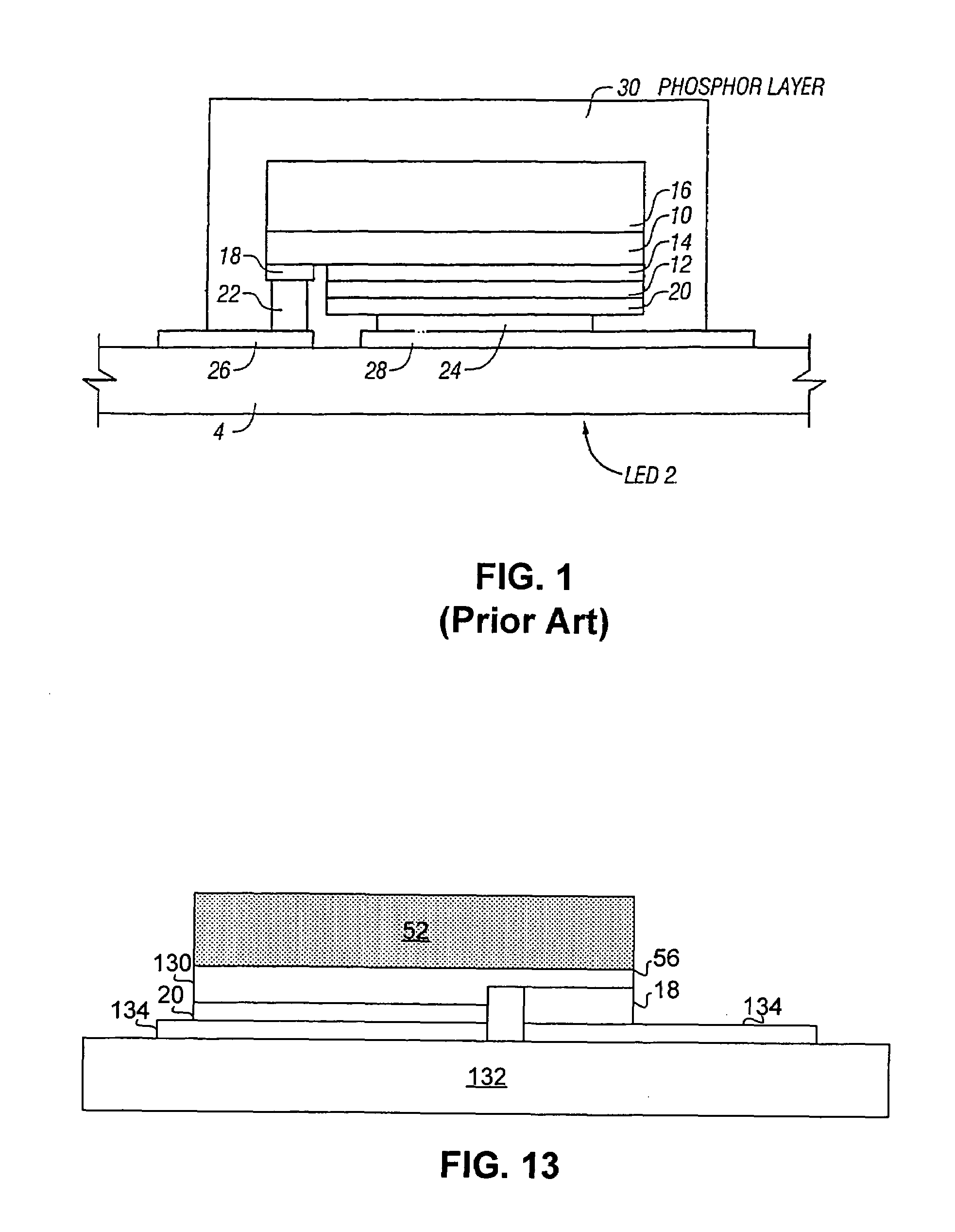
[0017]The prior art device illustrated in FIG. 1 includes a layer 30 bearing a phosphor. Phosphors are luminescent materials that can absorb an excitation energy (usually radiation energy), then emit the absorbed energy as radiation of a different energy than the initial excitation energy. State-of-the-art phosphors have quantum efficiencies near 100%, meaning nearly all photons provided as excitation energy are reemitted by the phosphor. State-of-the-art phosphors are also highly absorbent. If a light emitting device can emit light directly into such a highly efficient, highly absorbent phosphor, the phosphor may efficiently extract light from the device, reducing the optical losses described above.

[0018]The device illustrated in FIG. 1 does not exploit these properties of phosphor. In the device illustrated in FIG. 1, substrate 16 separates phosphor layer 30 from the III-nitride device regions 10, 12, and 14. As described above, much light is trapped within the semiconductor layer...


PUM

PropertyMeasurementUnit
thicknessaaaaaaaaaa
pressureaaaaaaaaaa
temperatureaaaaaaaaaa

Abstract

A material such as a phosphor is optically coupled to a semiconductor structure including a light emitting region disposed between an n-type region and a p-type region, in order to efficiently extract light from the light emitting region into the phosphor. The phosphor may be phosphor grains in direct contact with a surface of the semiconductor structure, or a ceramic phosphor bonded to the semiconductor structure, or to a thin nucleation structure on which the semiconductor structure may be grown. The phosphor is preferably highly absorbent and highly efficient. When the semiconductor structure emits light into such a highly efficient, highly absorbent phosphor, the phosphor may efficiently extract light from the structure, reducing the optical losses present in prior art devices.

Description

BACKGROUND[0001]1. Field of Invention[0002]The present invention relates to wavelength converted semiconductor light emitting devices.[0003]2. Description of Related Art[0004]Semiconductor light-emitting devices including light emitting diodes (LEDs), resonant cavity light emitting diodes (RCLEDs), vertical cavity laser diodes (VCSELs), and edge emitting lasers are among the most efficient light sources currently available. Materials systems currently of interest in the manufacture of high-brightness light emitting devices capable of operation across the visible spectrum include Group III-V semiconductors, particularly binary, ternary, and quaternary alloys of gallium, aluminum, indium, and nitrogen, also referred to as III-nitride materials, and binary, ternary, and quaternary alloys of gallium, aluminum, indium, and phosphorus, also referred to as III-phosphide materials. Typically, III-nitride light emitting devices are fabricated by epitaxially growing a stack of semiconductor l...

Claims


Application Information

Patent Timeline
Patent Type & Authority Patents(United States)
IPC IPC(8): H01L21/00H01L33/00H01L33/50
CPCB82Y30/00C04B35/44C04B35/495C04B35/6268C04B35/62805C04B35/62807C04B35/62813C04B35/645C04B37/001C04B37/005C04B37/006C04B37/008C04B37/026H01L33/501H01L2924/0002C04B2235/3217C04B2235/3225C04B2235/3229C04B2235/5454C04B2237/02C04B2237/06C04B2237/064C04B2237/068C04B2237/08C04B2237/083C04B2237/10C04B2237/12C04B2237/30C04B2237/34C04B2237/343C04B2237/36C04B2237/363C04B2237/365C04B2237/366C04B2237/368C04B2237/52C04B2237/525C04B2237/704C04B2237/708C04B2237/76H01L33/0079H01L33/08H01L2924/00H01L2224/14H01L2224/05573H01L2224/05568H01L2924/00014H01L2224/0554H01L33/0093H01L2224/05599H01L2224/0555H01L2224/0556H01L33/50
Inventor KRAMES, MICHAEL R.MUELLER, GERD O.
Owner LUMILEDS
Why Eureka
Try Eureka