

Organic electroluminescent element
a technology of electroluminescent elements and organic materials, which is applied in the direction of organic chemistry, organic semiconductor devices, luminescent compositions, etc., can solve the problems of improving efficiency and problematic fluorescence emission, and achieve the effects of reducing a drive voltage, improving luminous efficiency, and low drive voltag
- Summary
- Abstract
- Description
- Claims
- Application Information
AI Technical Summary
Benefits of technology
Problems solved by technology
Method used
Image

Examples
first exemplary embodiment
Arrangement(s) of Organic EL Device
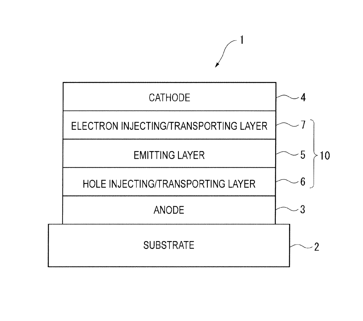
[0050]An arrangement of an organic EL device according to a first exemplary embodiment will be described.
[0051]The organic EL device according to the first exemplary embodiment includes a pair of electrodes and an organic layer between the pair of electrodes. The organic layer includes one or more layers formed of an organic compound. The organic layer may further include an inorganic compound.
[0052]In the organic EL device according to the exemplary embodiment, at least one layer of the organic layer is an emitting layer. Accordingly, the organic layer may be provided by a single emitting layer. Alternatively, the organic layer may be provided by layers employed in an organic EL device such as a hole injecting layer, a hole transporting layer, an electron injecting layer, an electron transporting layer, a hole blocking layer, and an electron blocking layer.
[0053]Representative arrangement examples of the organic EL device are as follows:
(a) anode / ...
second exemplary embodiment
[0334]Arrangement(s) of an organic EL device according to a second exemplary embodiment will be described. In the description of the second exemplary embodiment, the same components as those in the first exemplary embodiment are denoted by the same reference signs and names to simplify or omit an explanation of the components. In the second exemplary embodiment, the same materials and compounds as described in the first exemplary embodiment are usable unless particularly described.
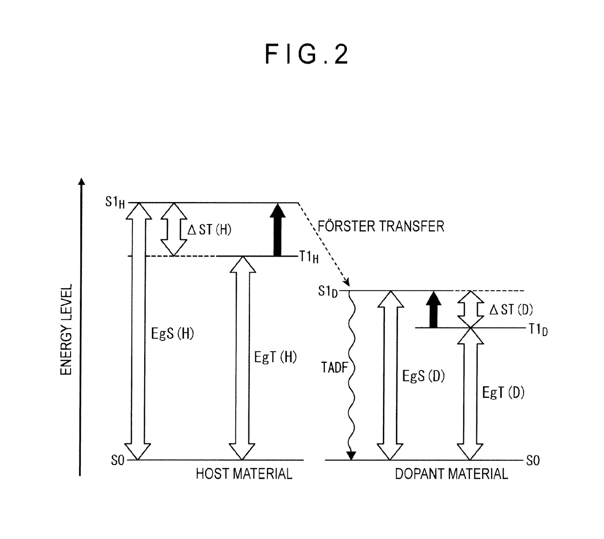
[0335]The organic EL device in the second exemplary embodiment has the same device arrangement as in the first exemplary embodiment, in which the host material and the dopant material contained in the emitting layer has a specific value of ΔST. Specifically, a difference ΔST(H) between singlet energy EgS(H) of the host material and an energy gap Eg77K(H) at 77K of the host material satisfies a numerical formula (Numerical Formula 1) below. Further, a difference ΔST(D) between singlet energy EgS(D) of the d...
third exemplary embodiment
[0364]Arrangements) of an organic EL device according to a third exemplary embodiment will be described. In the description of the third exemplary embodiment, the same components as those in the first exemplary embodiment are denoted by the same reference signs and names to simplify or omit an explanation of the components. In the third exemplary embodiment, the same materials and compounds as described in the above exemplary embodiments are usable unless particularly described.
[0365]The organic EL device in the third exemplary embodiment has the same device arrangement as in the first exemplary embodiment, except that the compound represented by the formula (1) is represented by a formula (40) below. The compound represented by the formula (40) below is contained in the emitting layer. As for other points, the organic EL device according to the third exemplary embodiment is the same as the organic EL device according to the above exemplary embodiments.
[0366]
[0367]In the formula (40...
PUM
| Property | Measurement | Unit |
|---|---|---|
| internal quantum efficiency | aaaaa | aaaaa |
| internal quantum efficiency | aaaaa | aaaaa |
| internal quantum efficiency | aaaaa | aaaaa |
Abstract
Description
Claims
Application Information