
Scan systems and methods

a scan system and scanner technology, applied in the field of array scan systems and methods, can solve the problems of complicated addition of scan testing capabilities to a system, often problematic traditional attempts at addressing these challenges, and undesirable impacts, and achieve the effect of facilitating efficient and effective scan operations

Active Publication Date: 2018-02-06
NVIDIA CORP
View PDF20 Cites 0 Cited by
  • Summary
  • Abstract
  • Description
  • Claims
  • Application Information

AI Technical Summary

Benefits of technology

This patent describes a system and method for efficiently and effectively scanning components. The system includes a component that can be scanned or viewed as a whole, rather than individually. This component can be combined with other components to form a scannable component that can be used in a variety of functions or operations, such as regular data operations, scan operations, controllability, and fault detection. Overall, this system provides a flexible and efficient way to scan components in a wide range of applications.

Problems solved by technology

However, adding scan testing capabilities to a system can be complicated and also have undesirable impacts.
However, traditional array approaches that include structured data paths usually have some characteristics that present challenges for scan testing (e.g., challenges related to ATPG tools, diagnosibility, etc.).
Traditional attempts at addressing these challenges are often problematic.
While scan testability typically has a variety of benefits it can also often have associated potential undesirable impacts.
Adding scan testability can have detrimental impacts on timing and typically increases the size of the circuitry.
There is usually a trade off between adding scan testability and the undesirable impacts.
Leaving out or limiting scan test components typically leads to reduced ability to detect faults.

Method used


Image

  • Scan systems and methods
  • Scan systems and methods
  • Scan systems and methods

Examples


Embodiment Construction

[0017]Reference will now be made in detail to the preferred embodiments of the invention, examples of which are illustrated in the accompanying drawings. While the invention will be described in conjunction with the preferred embodiments, it will be understood that they are not intended to limit the invention to these embodiments. On the contrary, the invention is intended to cover alternatives, modifications and equivalents, which may be included within the spirit and scope of the invention as defined by the appended claims. Furthermore, in the following detailed description of the present invention, numerous specific details are set forth in order to provide a thorough understanding of the present invention. However, it will be obvious to one of ordinary skill in the art that the present invention may be practiced without these specific details. In other instances, well known methods, procedures, components, and control component under analysis have not been described in detail as...


PUM


Abstract

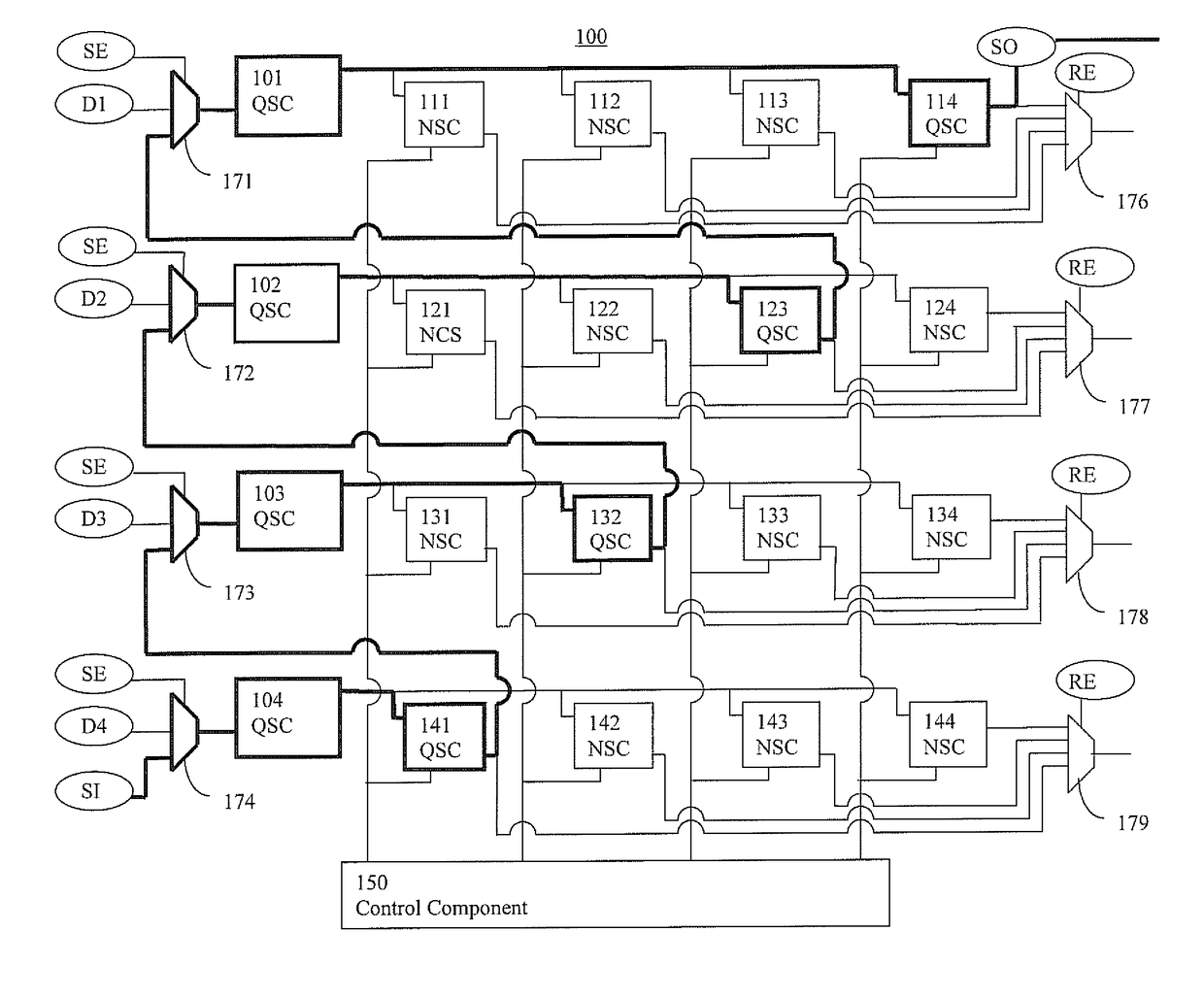
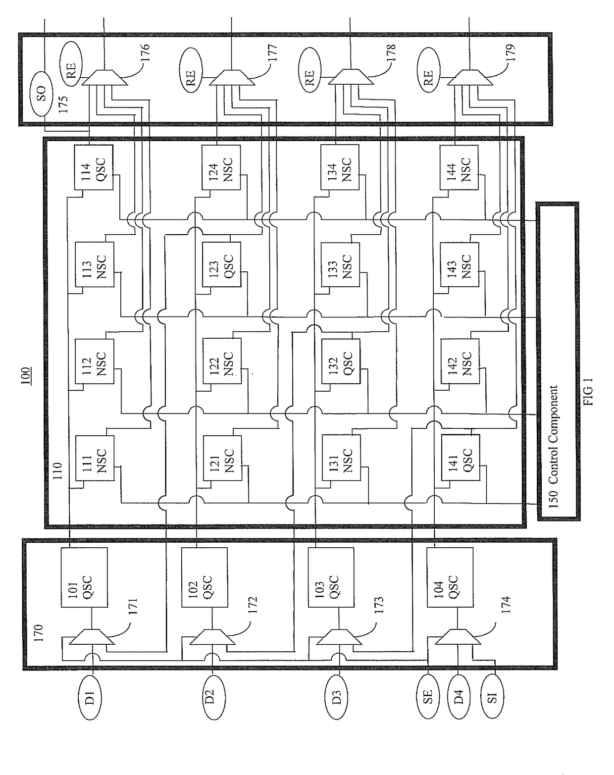
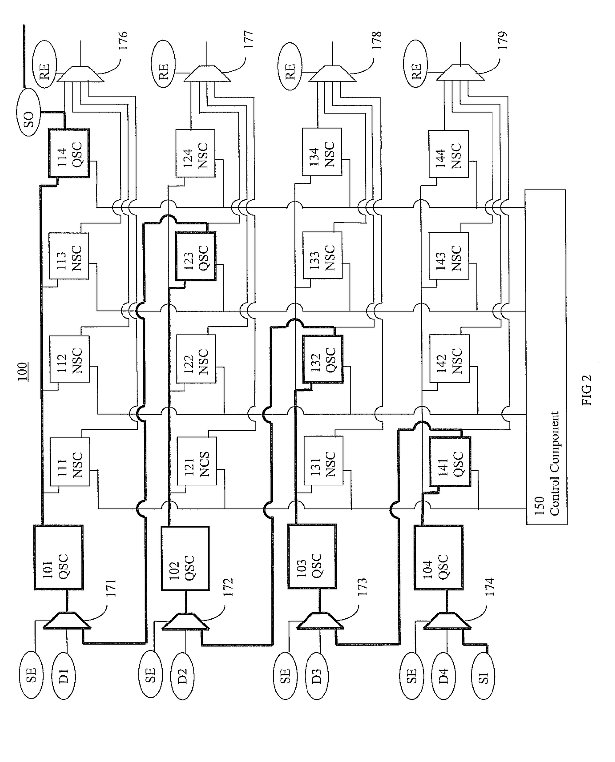
Efficient scan system presented can comprise: an array including a plurality of array non scannable components and a plurality of array quasi-scannable components wherein each column of the array includes at least one of the plurality of array quasi-scannable components; and an input interface configured to receive and selectively forward data and scan information to at least a portion of the array. At least a portion of the plurality of array quasi-scannable components can form a diagonal pattern in the array. The input interface can include: an input interface selection component wherein an output of the input interface selection component is communicatively coupled to an input of the input interface quasi-scannable component associated with one row and an input of the input interface selection component is communicatively coupled to an output of one of the plurality of array quasi-scannable components associated with another row.

Description

FIELD OF THE INVENTION[0001]The present invention relates to scan systems and methods. In particular, the present invention relates to array scan systems and methods.BACKGROUND OF THE INVENTION[0002]Electronic systems and devices have made a significant contribution towards the advancement of modern society and are utilized in a number of applications to achieve advantageous results. Numerous electronic technologies such as digital computers, calculators, audio devices, video equipment, and telephone systems have facilitated increased productivity and reduced costs in analyzing and communicating data in most areas of business, science, education and entertainment. These electronic systems typically include various components and scan testing the system components is often important for ensuring proper testing and debug. However, adding scan testing capabilities to a system can be complicated and also have undesirable impacts.[0003]Some conventional systems include arrays of componen...

Claims


Application Information

Patent Timeline
Patent Type & Authority Patents(United States)
IPC IPC(8): G01R31/3185G01R31/3177
CPCG01R31/3177G01R31/318586
Inventor SANGHANI, AMITGOLSHAN, FARIDEHKOTTAPALLI, VENKATASONAWANE, MILINDKULKARNI, KETAN
Owner NVIDIA CORP
Learn More