

Light emitting device
a technology of light emitting device and light source, which is applied in the direction of semiconductor devices, basic electric elements, electrical apparatus, etc., can solve the problem of narrow orientation angle of the emitting device b>100/b>, and achieve the effect of improving the light output power
Active Publication Date: 2018-03-27
SUZHOU LEKIN SEMICON CO LTD
View PDF18 Cites 0 Cited by
- Summary
- Abstract
- Description
- Claims
- Application Information
AI Technical Summary
Benefits of technology
The patent relates to a light emitting device and package with an uneven surface structure on the substrate, which refracts light emitted from the device at a higher angle, resulting in a wider orientation angle and increased light output power. The uneven surface structure can be present in the edge region or the central region of the transmissive conductive layer, allowing for higher refraction angle in the desired location.
Problems solved by technology
Furthermore, there may be a problem in that the light emitting device 100 has a narrow orientation angle.
Method used
View moreImage
Smart ImageViewing Examples

Examples
Embodiment Construction
[0141]Various embodiments have been described in the best mode for carrying out the invention.
INDUSTRIAL APPLICABILITY
[0142]The above-described light emitting device package is applicable to various fields. For example, the light emitting device package is applicable to a lighting apparatus. For example, the lighting apparatus may include at least one of a backlight unit, a lighting unit, an indicator, a lamp and a street lamp.
Login to View More PUM
 Abstract
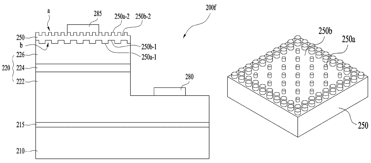
An embodiment provides a light-emitting element comprising: a substrate; a light-emitting structure, which is arranged on the substrate, and which comprises a first conductive semiconductor layer, an active layer, and a second conductive semiconductor layer; a light-transmissive conductive layer arranged on the second conductive semiconductor layer; and first and second electrodes electrically connected to the first and second conductive semiconductor layers, respectively, wherein the light-transmissive conductive layer has corrugated portions formed on a first surface thereof, which is directed to the second conductive semiconductor layer, and the density of the corrugated portions in the peripheral area of the light-transmissive conductive layer is larger than the density of the corrugated portions in the central area of the light-transmissive conductive layer.
Description
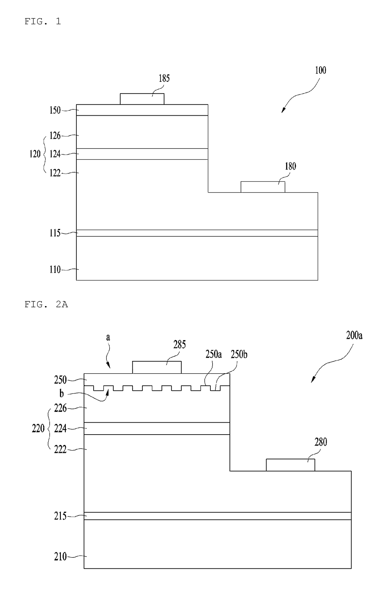
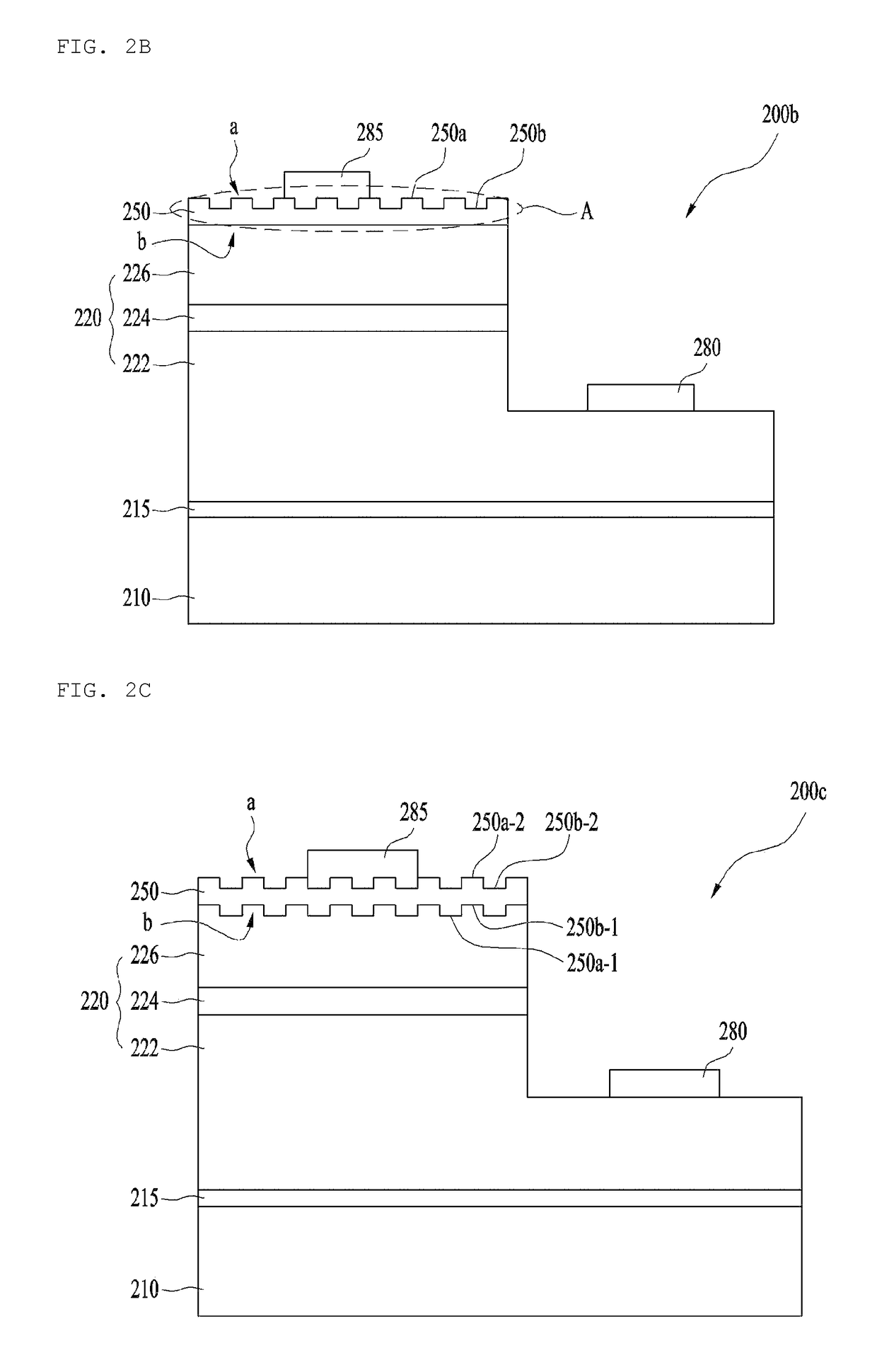
CROSS REFERENCE TO RELATED APPLICATIONS[0001]This application is the National Phase of PCT International Application No. PCT / KR2015 / 005933, filed on Jun. 12, 2015, which claims priority under 35 U.S.C. 119(a) to Patent Application No. 10-2014-0071459, filed in the Republic of Korea on Jun. 12, 2014, all of which are hereby expressly incorporated by reference into the present application.TECHNICAL FIELD[0002]Embodiments relate to a light emitting device and a light emitting device package including the same, and more particularly to a light emitting device having enhanced light extraction efficiency.BACKGROUND ART[0003]Group III-V compound semiconductors such as GaN and AlGaN are widely used in optoelectronics and for electronic devices by virtue of many advantages thereof, for example, wide and easy-adjustable band gap energy.[0004]In particular, light emitting devices, such as light emitting diodes (LEDs) and laser diodes, which use a Group III-V or Group II-VI compound semiconduct...
Claims
Login to View More Application Information
Patent Timeline
 Patent Type & AuthorityPatents(United States)
IPC IPC(8): H01L33/22H01L33/38H01L33/42
CPCH01L33/22H01L33/382H01L33/42H01L2224/48091H01L2224/49107H01L2924/181H01L2924/00012H01L2924/00014H01L33/20H01L2933/0016
InventorKIM, CHONG COOK
OwnerSUZHOU LEKIN SEMICON CO LTD