Multi-chip stacked devices

a technology of multi-chips and devices, applied in semiconductor devices, semiconductor/solid-state device details, electrical apparatus, etc., can solve the problem of primarily limited density of ic packages

Inactive Publication Date: 2000-03-14
ROUND ROCK RES LLC
View PDF13 Cites 265 Cited by
  • Summary
  • Abstract
  • Description
  • Claims
  • Application Information

AI Technical Summary

Benefits of technology

Other object, advantages, and capabilities of the present ...

Problems solved by technology

IC package density is primarily limited by the area...

Method used


Image

  • Multi-chip stacked devices
  • Multi-chip stacked devices

Examples


Embodiment Construction

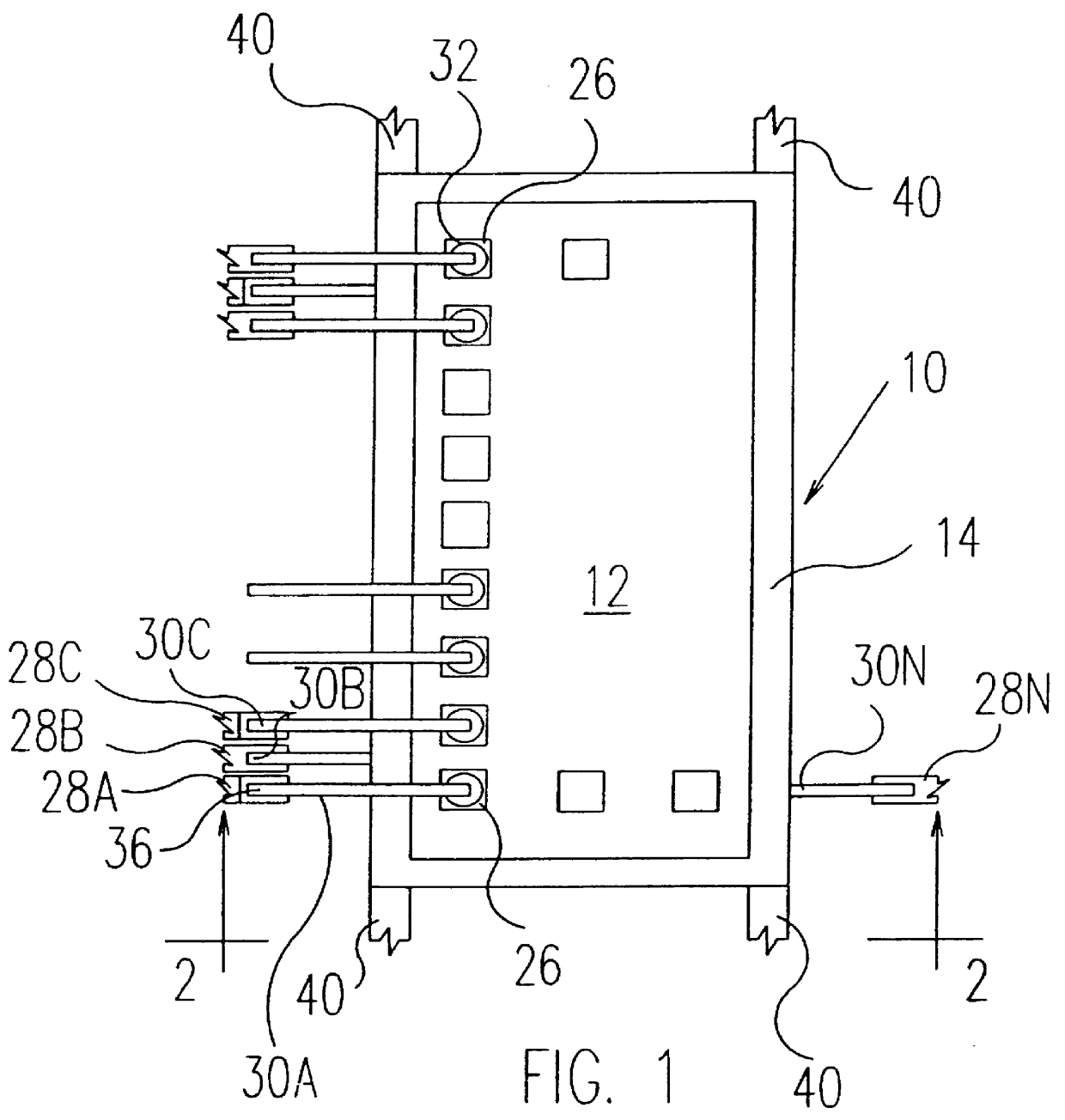
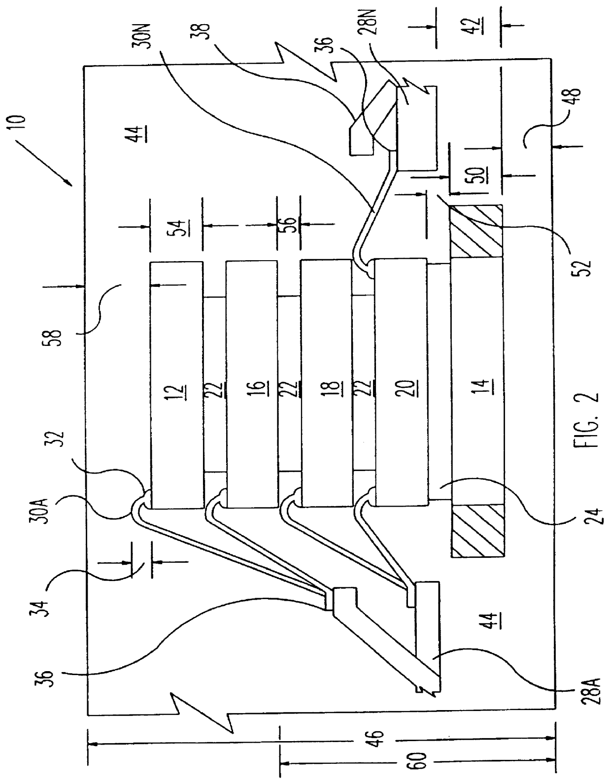
Referring to FIG. 1, the stacked die device 10 is shown prior to encapsulation disclosing the top die 12 mounted the paddle 14 and other dies 16, 18, and 20 (FIG. 2) which are adhesively connected to each other by a controlled-thickness thermoplastic-adhesive layer at 22. Thermoplastic indicating the adhesive sets at an elevated temperature. The group of four dies are attached to the paddle 14 by a controlled thin-adhesive layer 24.

Each of the die bonding pads 26 in double rows are electrically connected to multiple lead fingers 28A, 28B, 28C . . . 28N by thin (0.001 inch) gold or aluminum wires 30A, 30B, 30C . . . 30N; gold being the preferred metal. For clarity, only part of the 18 bonding pads, wires, and fingers are shown. The critical bonding method used at the die end pad 26 is ultrasonic ball bond as named by the shape of the bond as at 32. This first-installed bond and formed gold wire are low-loop wire bonds as seen at critical dimension 34, as will be described later.

The o...


PUM


Abstract

A multiple stacked die device is disclosed that contains up to four dies and does not exceed the height of current single die packages. Close-tolerance stacking is made possible by a low-loop-profile wire-bonding operation and thin-adhesive layer between the stacked dies.

Description

FIELD OF THE INVENTIONThis invention relates to a multiple die module that has a thickness the same or less than a standard package but has two or more stacked die, thereby increasing device density.BACKGROUND OF THE INVENTIONSemiconductor devices are typically constructed en masse on a silicon or gallium arsenide wafer through a process which comprises a number of deposition, masking, diffusion, etching, and implanting steps. When the devices are sawed into individual rectangular units, each takes the from of an integrated circuit (IC) die. In order to interface a die with other circuitry, it is (using contemporary conventional packaging technology) mounted on a lead frame paddle of a lead-frame strip which consists of a series of interconnected lead frames, typically ten in a row. The die-mounting paddle of a standard lead frame is larger than the die itself, and it is surrounded by multiple lead fingers of individual leads. The bonding pads of the die are then connected one by on...

Claims


Application Information

Patent Timeline
IPC IPC(8): H01L23/48H01L23/495H01L25/065
CPCH01L23/49551H01L23/49575H01L24/49H01L25/0657H01L24/45H01L2224/45124H01L2224/45144H01L2224/48091H01L2224/48247H01L2224/48465H01L2224/49175H01L2225/0651H01L2225/06575H01L2924/01005H01L2924/01006H01L2924/01013H01L2924/01014H01L2924/01031H01L2924/01079H01L2924/01082H01L2924/14H01L2924/00014H01L24/48H01L2924/00H01L2924/181H01L2224/05554H01L2924/00015H01L2224/05599H01L2924/00012
Inventor BALL, MICHAEL B.
Owner ROUND ROCK RES LLC
Why Eureka
Try Eureka