Method for manufacturing a solid-state image sensing device, such as a ccd

A technology of solid-state imaging element and manufacturing method, which is applied in the direction of electric solid-state devices, electrical components, semiconductor devices, etc., and can solve problems such as inability to reproduce colors

Inactive Publication Date: 2007-12-19
SANYO ELECTRIC CO LTD
View PDF5 Cites 0 Cited by
  • Summary
  • Abstract
  • Description
  • Claims
  • Application Information

AI Technical Summary

Problems solved by technology

This is especially the case with light generated by heat sources such as light bulbs, but color reproduction cannot be performed correctly

Method used


Image

  • Method for manufacturing a solid-state image sensing device, such as a ccd
  • Method for manufacturing a solid-state image sensing device, such as a ccd
  • Method for manufacturing a solid-state image sensing device, such as a ccd

Examples


Embodiment Construction

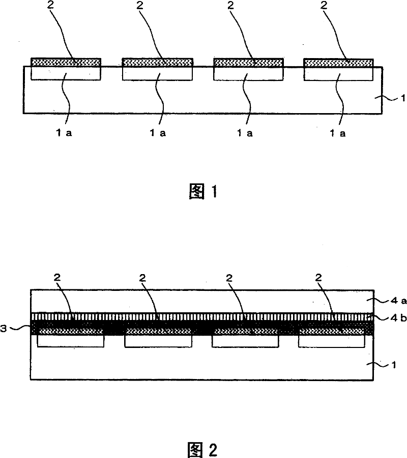
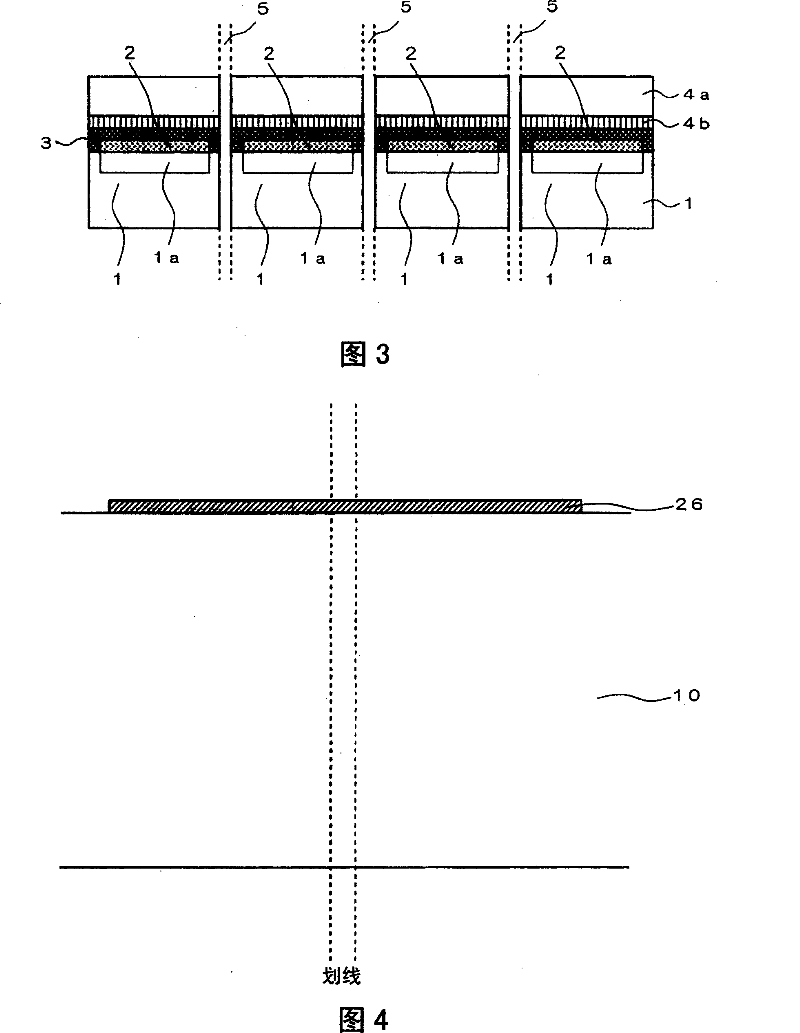
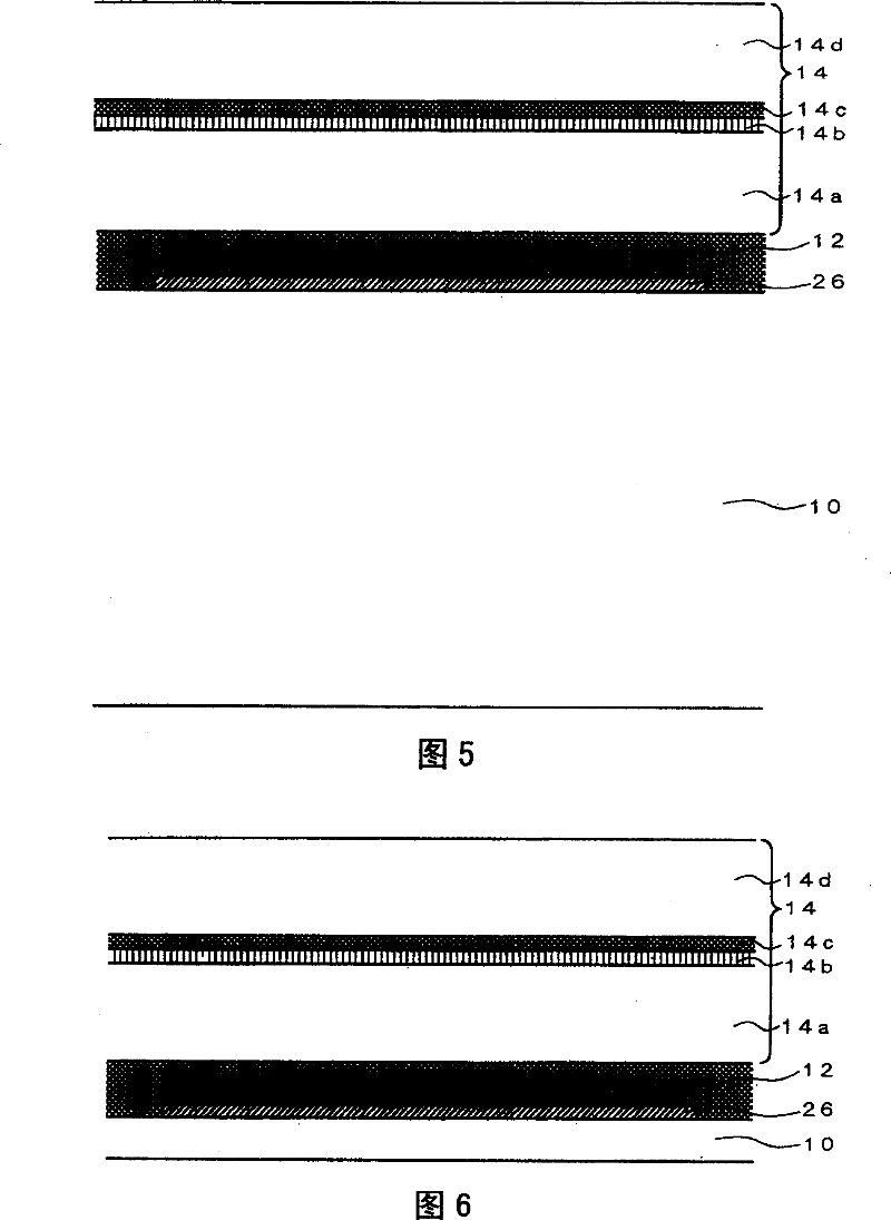
[0018] 1 to 3 are cross-sectional views showing the sequence of steps of the first embodiment of the method for manufacturing a solid-state imaging device according to the present invention. This embodiment is constituted by a light receiving element forming step, an infrared cut filter lamination step, and a dicing step.

[0019] First, in the light-receiving element forming step, as shown in FIG. 1 , a light-receiving element is formed in each region 1a divided by scribe lines on the surface of the semiconductor substrate 1 . The color filter 2 is stacked so as to cover the formation region 1 a of the light receiving element. The semiconductor substrate 1 can be made of common semiconductor materials such as silicon and gallium arsenide. For example, an integrated circuit of a CCD as a light receiving element can be formed by a well-known semiconductor process.

[0020] In the infrared cut filter lamination step, as shown in FIG. 2 , the infrared cut filter is bonded and fi...


PUM


Abstract

The present invention provides a method for making a solid imaging element that is equipped with an infrared beam cut filter without increasing any of assembly processes, wherein light receiving elements is formed upon every area (1a) that is divided by the scribe lines (5) of the semiconductor substrate (1), and the color filter (2) is laminated upon the areas (1a) that are formed with the light receiving elements. Further, a laminate attached with the infrared beam cut filter that deposited an infrared reflection film (4b) upon the surface of transparent substrate (4a), such as a glass or plastic piece, over the areas (1a) that are formed with the light receiving elements is formed by a resin layer (3) having light transmitting feature, such as epoxy adhesives. A large number of the solid imaging elements are made by severing the laminate along the scribe lines to separate the same into a number of independent solid imaging elements.

Description

technical field [0001] The present invention relates to solid-state imaging devices such as CCDs. Background technique [0002] An infrared cut filter is a device used to remove infrared components contained in incident light, and is a must-have device for color solid-state imaging devices generally used in TV cameras or digital cameras. If there is no such infrared ray blocking filter, since the incident light contains infrared rays, the solid-state imaging element 100 is sensitive to infrared rays, and the output of the solid-state imaging element 100 contains not only visible light but also infrared rays. error components. This is especially true for light generated by heat sources such as light bulbs, but accurate color reproduction cannot be performed. Contents of the invention [0003] As described above, in the conventional solid-state imaging device, the infrared cut filter is attached to the surface of the package, which increases the number of steps in the asse...

Claims


Application Information

Patent Timeline
Patent Type & Authority Patents(China)
IPC IPC(8): H01L27/146H01L27/148H01L31/09H01L27/14H01L31/00H04N5/335H04N5/357H04N5/369H04N5/372
CPCH01L27/14636H01L27/14687H01L27/14621H01L27/14831H01L27/1462H01L27/14685H01L31/02162
Inventor 小嶋数明浜田稔
Owner SANYO ELECTRIC CO LTD
Why Eureka
Try Eureka