Picture element structure and manufacturing method and storage capacitance structure therefor

A technology of pixel structure and manufacturing method, which is applied in semiconductor/solid-state device manufacturing, circuits, electrical components, etc., can solve the problems of easy leakage of stored electricity, and achieve the effects of improving easy leakage, wide use value, and difficult leakage

Active Publication Date: 2008-01-23
AU OPTRONICS CORP
View PDF2 Cites 0 Cited by
  • Summary
  • Abstract
  • Description
  • Claims
  • Application Information

AI Technical Summary

Problems solved by technology

[0008] The purpose of the present invention is to overcome the defects of the existing pixel structure and provide a new pixel structure. The technical problem to be solved is to improve the existing known metal layer-insulator layer-metal layer (MIM ) structure of the storage capacitor is easy to leak, so as to increase the value of the storage capacitor, which is more suitable for practical use

Method used


Image

  • Picture element structure and manufacturing method and storage capacitance structure therefor
  • Picture element structure and manufacturing method and storage capacitance structure therefor
  • Picture element structure and manufacturing method and storage capacitance structure therefor

Examples


Embodiment Construction

[0067] In order to further explain the technical means and effects of the present invention to achieve the intended purpose of the invention, the specific implementation methods, The structure, manufacturing method, steps, features and functions thereof are described in detail below.

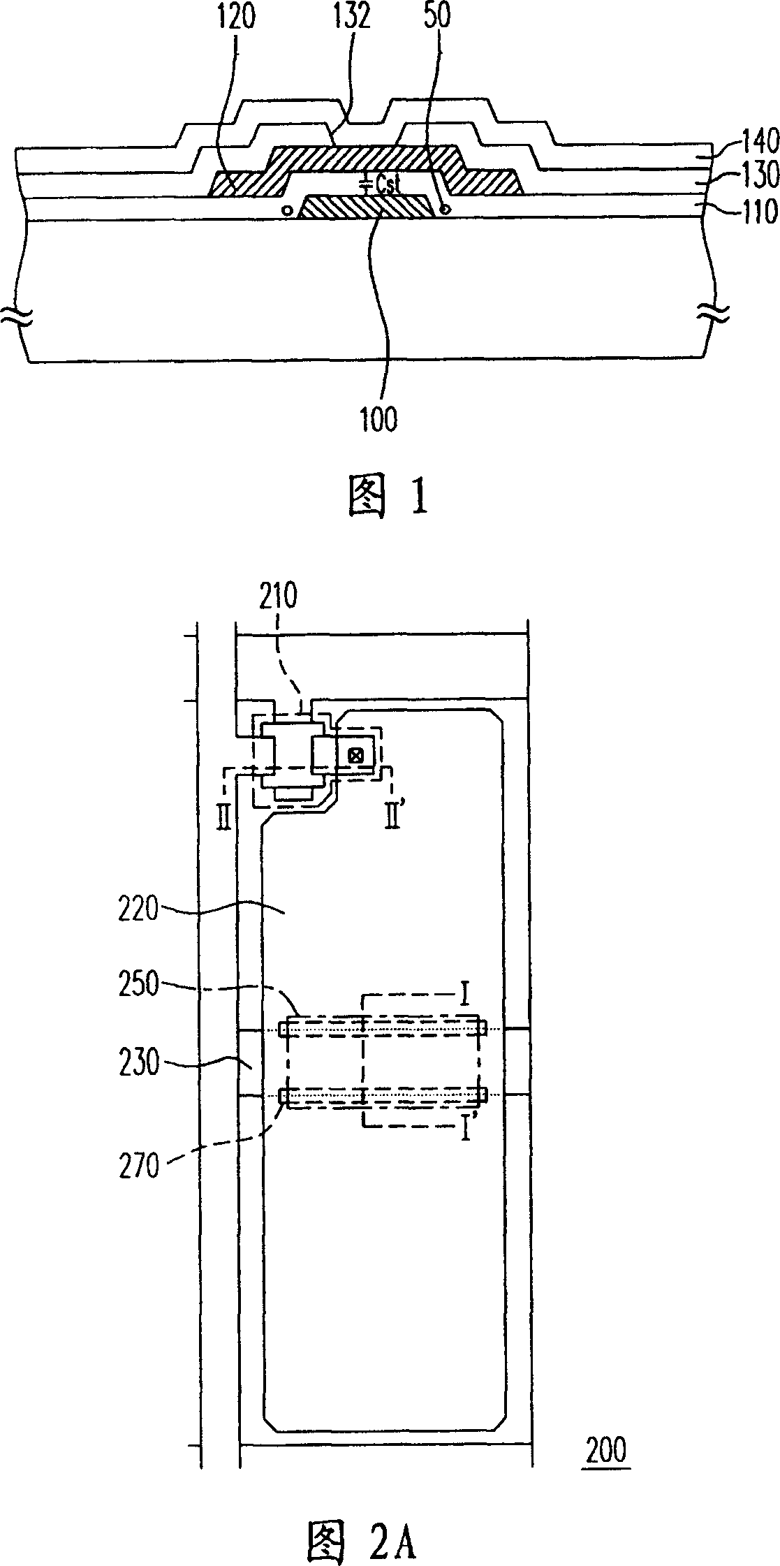
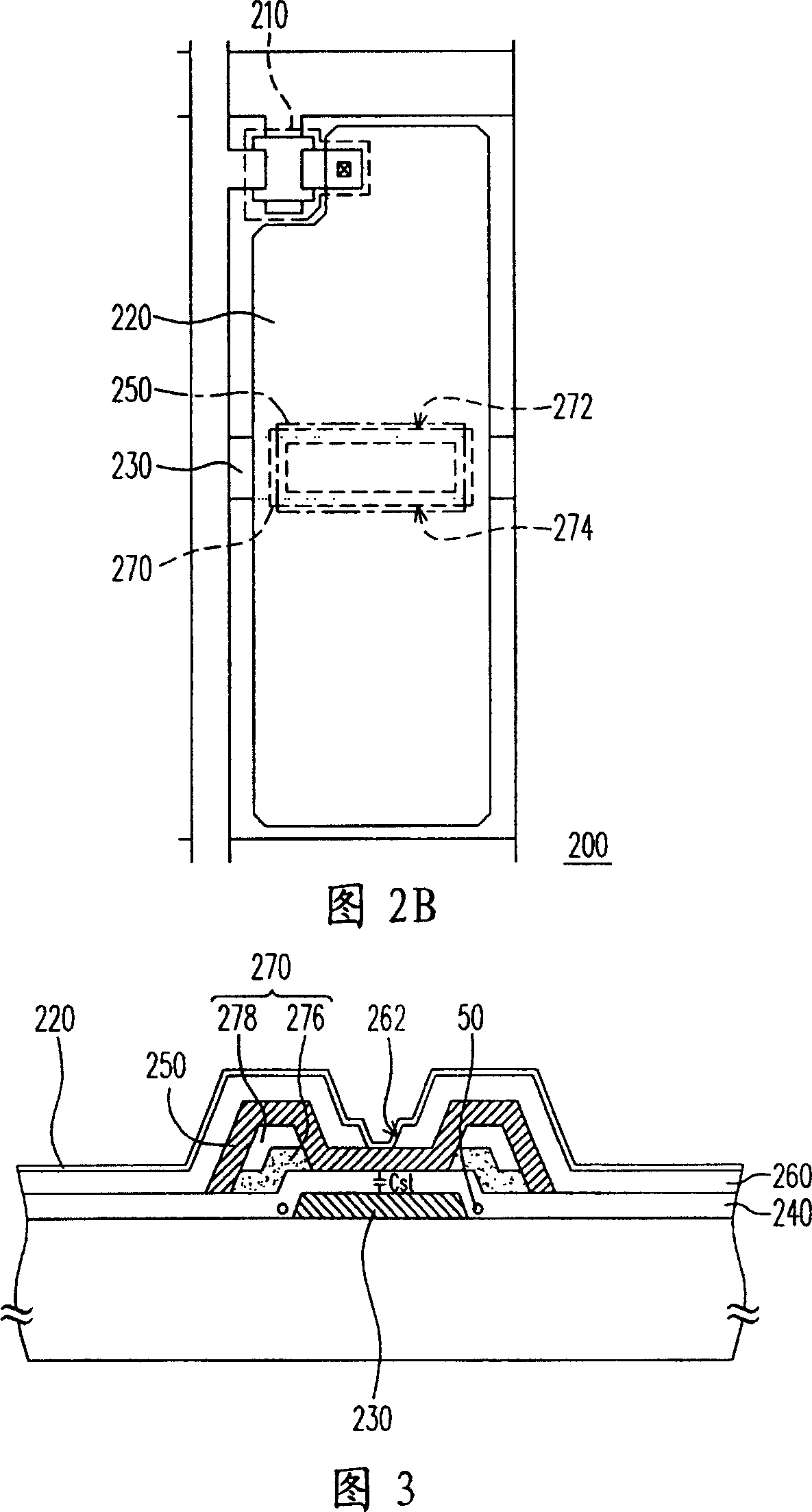
[0068] Please refer to FIG. 2A and FIG. 3 at the same time. FIG. 2A is a top view of a pixel structure according to a preferred embodiment of the present invention, and FIG. 3 is a cross-sectional view of line I-I' in FIG. 2A. The pixel structure 200 of the preferred embodiment of the present invention includes an active device 210 , a pixel electrode 220 , a lower electrode 230 , a gate insulating layer 240 , an upper electrode 250 , a protection layer 260 and a leakage current suppression layer 270 . The pixel electrode 220 is electrically connected to the active device 210 , and the lower electrode 230 is disposed below the pixel electrode 250 . In addition, the gate insulating layer 240 ext...


PUM


Abstract

This invention relates to a picture element structure and its process method and storage capacitor structure. The picture element structure comprises one driving part, picture element electrode, down electrode, upper electrode, and protective layer and leakage current suppressor layer. The picture element electrode is connected with the driving part and the down electrode is aligned down the picture electrode. The isolation layer stretches from the driving part into the picture element electrode bottom to cover the down electrode. The upper electrode is set on the isolation layer and is electrically connected with the picture element electrode. This invention also provides a picture element structure process method.

Description

technical field [0001] The present invention relates to a structure of a semiconductor device and a manufacturing method thereof, in particular to a pixel structure of a liquid crystal display (LCD) and a manufacturing method thereof. Background technique [0002] The rapid progress of the multimedia society is mostly due to the rapid progress of semiconductor devices or display devices. As far as displays are concerned, cathode ray tubes (cathode ray tubes, CRTs) have been monopolizing the display market in recent years due to their excellent display quality and economical efficiency. However, for the environment where individuals operate most terminals / display devices on the table, or from the perspective of environmental protection, if the trend of energy saving is predicted, cathode ray tubes still have many problems in terms of space utilization and energy consumption, and There is no effective solution to the demands of lightness, thinness, shortness, smallness and lo...

Claims


Application Information

Patent Timeline
Patent Type & Authority Patents(China)
IPC IPC(8): G02F1/136G02F1/133H01L21/00
Inventor 来汉中
Owner AU OPTRONICS CORP
Why Eureka
Try Eureka