Capacitor array for increasing memory capacitance on semiconductor base plate

A technology for capacitors and semiconductors, applied to the field of capacitor arrangement for increasing storage capacitance in semiconductor substrates

Inactive Publication Date: 2008-02-13
INFINEON TECH AG
View PDF4 Cites 0 Cited by
  • Summary
  • Abstract
  • Description
  • Claims
  • Application Information

AI Technical Summary

Problems solved by technology

[0006] Knowing that for feature sizes less than 100 nm, the capacitance of capacitors currently used in commercial microchips can only be increased by values ​​typically below 50% for predetermined cross-sectional segments

Method used


Image

  • Capacitor array for increasing memory capacitance on semiconductor base plate
  • Capacitor array for increasing memory capacitance on semiconductor base plate
  • Capacitor array for increasing memory capacitance on semiconductor base plate

Examples


Embodiment Construction

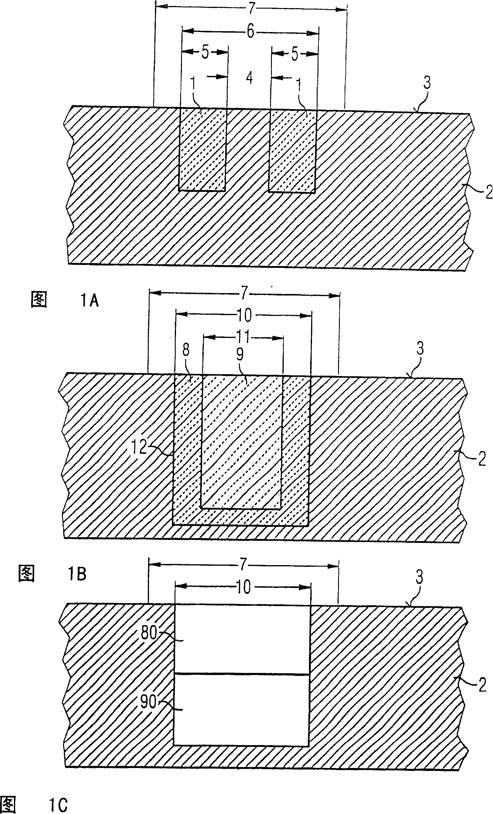
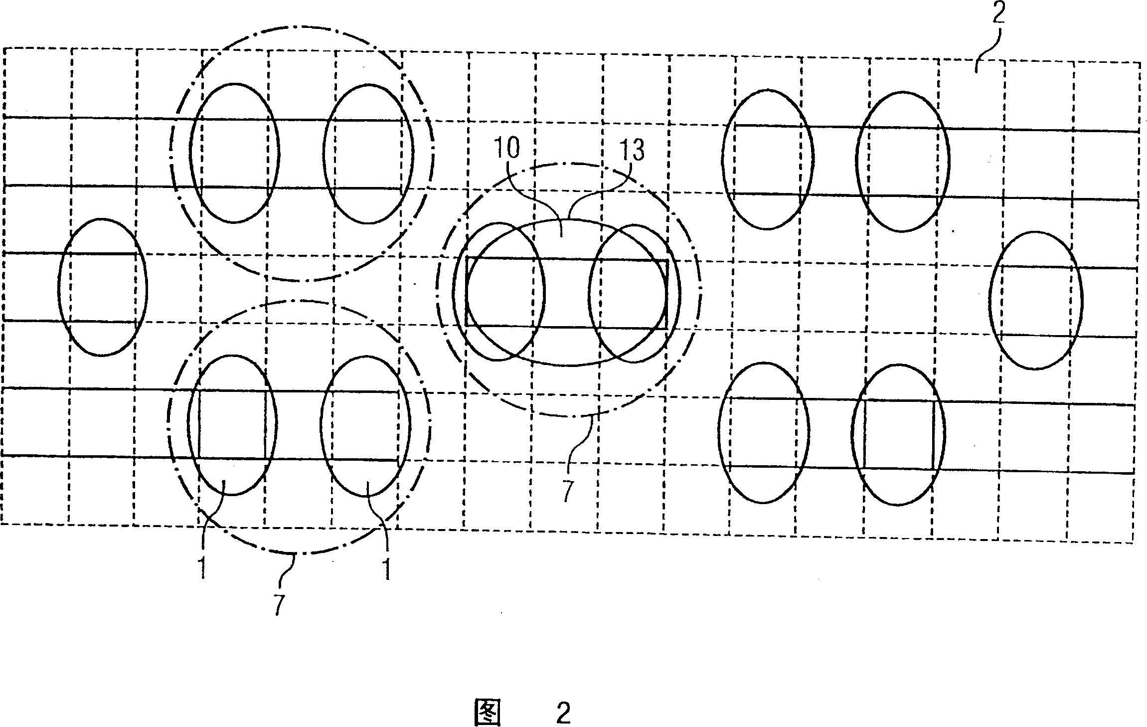
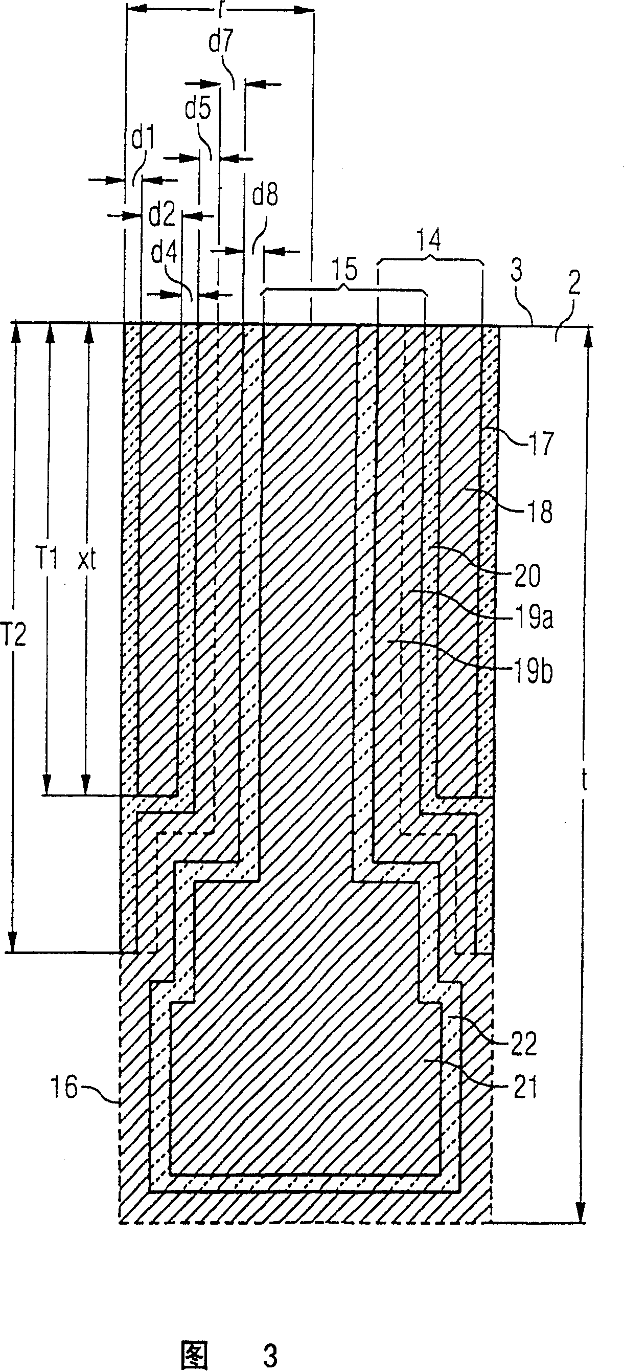
[0112]1A-1C show the arrangement of two capacitors 1 on a semiconductor substrate 2 , in this case the capacitors 1 are embodied as trench capacitors, ie they extend below the substrate surface 3 into the depth of the substrate 2 . For clarity of illustration, the description does not show the components required to drive the capacitor 1, such as selection transistors and corresponding intermediate connections. Likewise, without a detailed description of the individual layers of the capacitor 1, such as electrode layers and dielectric layers, the capacitor 1 has a distance 4 and also a diameter 5, which means that at least the area 6 occupied by two capacitors 1 results in the on the surface 3 of the substrate 2. In order to obtain the area requirement for the arrangement of the two capacitors 1, the minimum distance to the adjacent capacitor or the memory cell must also be taken into consideration, so the area 7 is obtained as the area requirement. If the area 7 is to be redu...


PUM


Abstract

Arrangement of capacitors which, without taking up an additional area in the semiconductor substrate (2), have an increased capacitance compared with conventional capacitors in DRAM memory cells. The arrangement of capacitors (8,9) according to the invention is based on a combination of two or more separately arranged individual capacitors in or on a substrate (2) to form two or more capacitors arranged one in the other or one above the other. In this case, an outer capacitor (8) encloses at least one or a plurality of inner capacitors (9) or a substantial part of an upper capacitor lies above a lower capacitor. A method for fabricating the arrangement of capacitors also is described.

Description

technical field [0001] The invention relates to an arrangement of at least two capacitors in or on a semiconductor substrate and to a method of manufacturing the capacitors. Background technique [0002] A large number of DRAM (Dynamic Random Access Memory) modules are manufactured and used in many fields. The new generation of DRAM modules needs to have a smaller size on the one hand and, on the other hand, a larger number of memory cells to store Data, ie increased storage density, creates a need to further reduce the cell size of the individual memory cells, including storage capacitors and select transistors. A distinction is made between "trench capacitor" and "stack capacitor" types of memory cells, depending on whether the storage capacitor is arranged in the silicon substrate or below the transistor for driving purposes or above the substrate surface or above the transistor. [0003] In the case of a memory cell of the "trench capacitor" type, a trench is formed in ...

Claims


Application Information

Patent Timeline
Patent Type & Authority Patents(China)
IPC IPC(8): H01L27/108H01L21/8242H01G4/228H01L21/334H01L29/94
CPCH01L29/945H01L29/66181
Inventor M·古特斯彻H·塞德尔
Owner INFINEON TECH AG
Why Eureka
Try Eureka