
Picture-element electrode switch element and manufacturing method thereof

A pixel electrode and switching element technology, which is applied in the field of thin film transistor switching elements and its manufacturing, can solve problems affecting the reliability of TFT-LCD, and achieve the effect of preventing copper gate diffusion

Active Publication Date: 2008-02-27
AU OPTRONICS CORP
View PDF8 Cites 0 Cited by
  • Summary
  • Abstract
  • Description
  • Claims
  • Application Information

AI Technical Summary

Problems solved by technology

Moreover, copper is easy to diffuse and form copper silicide with silicon, which seriously affects the reliability of TFT-LCD

Method used


Image

  • Picture-element electrode switch element and manufacturing method thereof
  • Picture-element electrode switch element and manufacturing method thereof
  • Picture-element electrode switch element and manufacturing method thereof

Examples


no. 1 example

[0026] According to a preferred embodiment of the present invention, the method includes the following main steps.

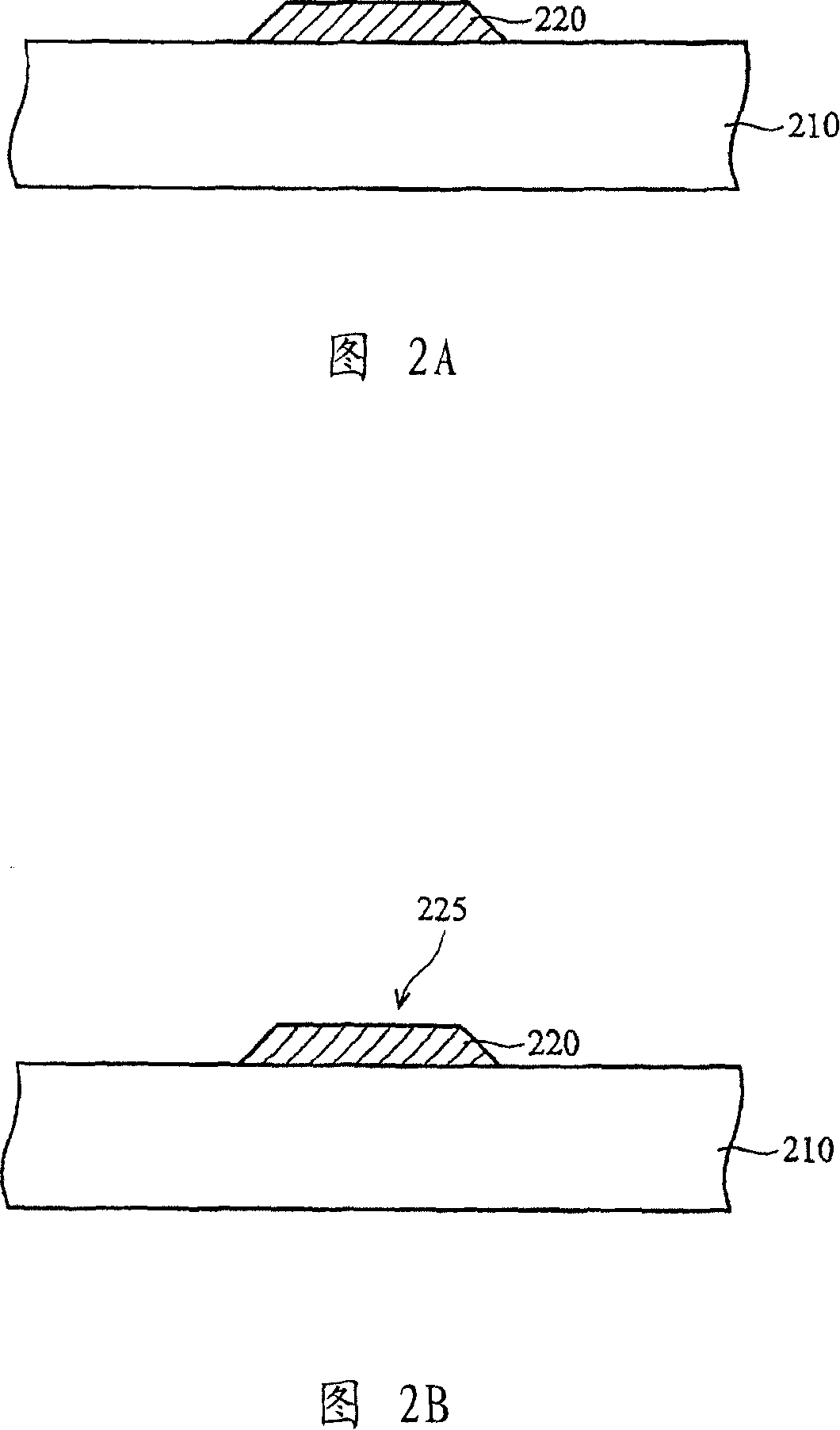
[0027] As shown in FIG. 2A, a copper layer (not shown) is formed by chemical vapor deposition, electrochemical plating (ECP) or physical vapor deposition, and then a photolithographic etching process is performed to form a gate 220 on the above a substrate 210 . The substrate 210 includes a glass substrate. The gate 220 includes copper and has a thickness between about 100 and 500 nanometers.

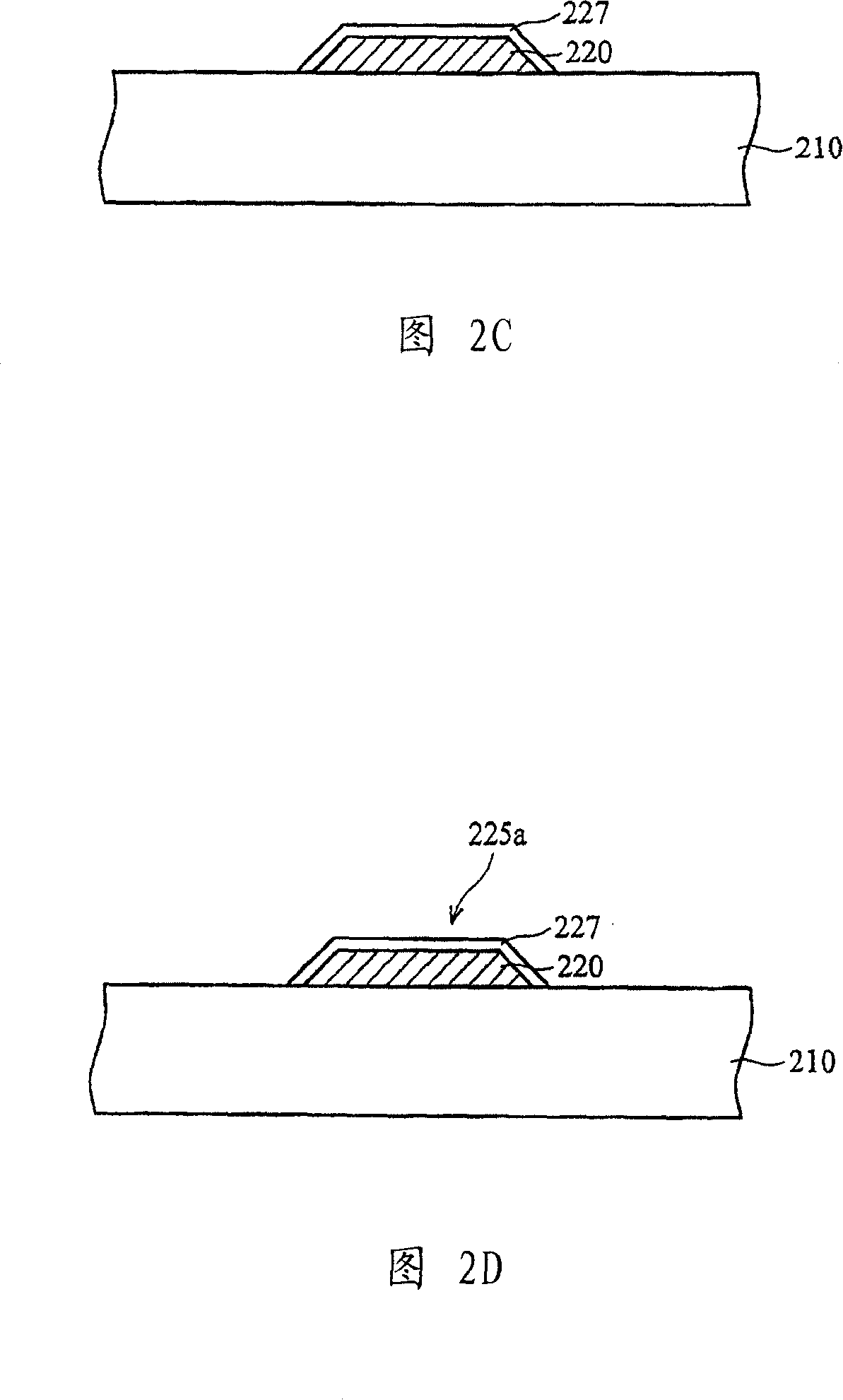
[0028] As shown in FIGS. 2B and 2C, a plasma treatment 225 is performed on the surface of the gate 220 to conformably form a first copper silicide layer 227 (CuSi x ) above the gate 220. Wherein, the plasma treatment 225 is carried out in a reaction chamber containing silane gas at a temperature of 180-370° C., and the silicon in the silane reacts with the surface of the gate 220 composed of copper to produce a first copper silicide layer 227 for use in Copper is prev...

no. 2 example

[0033] According to another preferred embodiment of the present invention, the method of the present invention includes the following steps.

[0034] As shown in FIG. 3A, a copper layer (not shown) is formed by chemical vapor deposition or electrochemical plating (ECP) or physical vapor deposition, followed by a photolithographic etching process to form a grid 220 on a above the substrate 210 . The substrate 210 includes a glass substrate. The gate 220 includes copper and has a thickness between about 100 and 500 nanometers.

[0035] As shown in FIGS. 3B and 3C, a plasma treatment 225 is performed on the surface of the gate 220 to conformably form a first copper silicide layer 227 (CuSi x ) above the gate 220. Wherein, the plasma treatment 225 is carried out in a reaction chamber containing silane gas at a temperature of 180-370° C., and the silicon in the silane reacts with the surface of the gate 220 composed of copper to produce a first copper silicide layer 227 for use ...


PUM

PropertyMeasurementUnit
thicknessaaaaaaaaaa

Abstract

The method includes steps: forming a gate pole on a base plate; forming a first layer of copper silicide on the gate pole; forming a insulating layer on the first layer of copper silicide; forming a semiconductor layer on the insulating layer; forming a source pole / drain pole on the semiconductor layer. Moreover, the method also includes procedure: forming a second layer of copper silicide on the semiconductor layer, and the second layer of copper silicide is located between the semiconductor layer and the source pole / drain pole.

Description

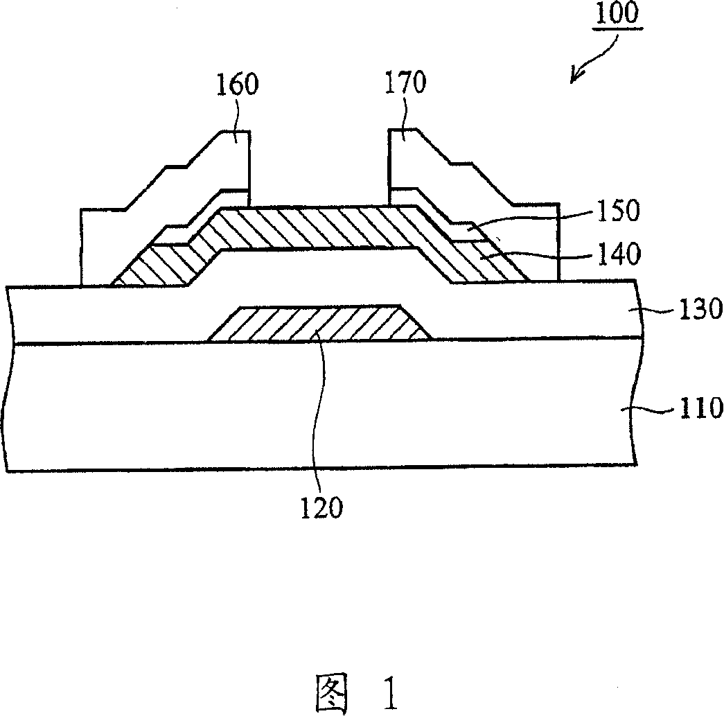
technical field [0001] The invention relates to a switch element, in particular to a thin film transistor switch element and a manufacturing method thereof. Background technique [0002] Bottom-gate type thin film transistor devices have been widely used in thin film transistor liquid crystal displays (TFT-LCDs). Please refer to FIG. 1 , which shows a conventional bottom-gate TFT structure 100 . The TFT structure 100 includes a substrate 110 , a gate 120 , an insulating layer 130 , a channel layer 140 , an ohmic contact layer 150 and a source / drain layer 160 / 170 . [0003] As the size of the TFT-LCD increases, the metal gate line including the gate of the thin film transistor must meet the requirement of low resistance. Since copper and copper alloy materials have relatively low electrical resistance, they are the best choices for gate materials. [0004] However, in the subsequent plasma process, copper often reacts with some free radicals and generates copper oxide, t...

Claims


Application Information

Patent Timeline
Patent Type & Authority Patents(China)
IPC IPC(8): H01L21/3205
Inventor 方国龙蔡文庆李永祥林汉涂
Owner AU OPTRONICS CORP
Learn More