Circuit arrangement for generating switching signal for current controlled switched mode power supply
A switching power supply and switching signal technology, applied in the field of circuits, can solve the problems of easy thermal overload and damage of loads
- Summary
- Abstract
- Description
- Claims
- Application Information
AI Technical Summary
Problems solved by technology
Method used
Image

Examples
Embodiment Construction
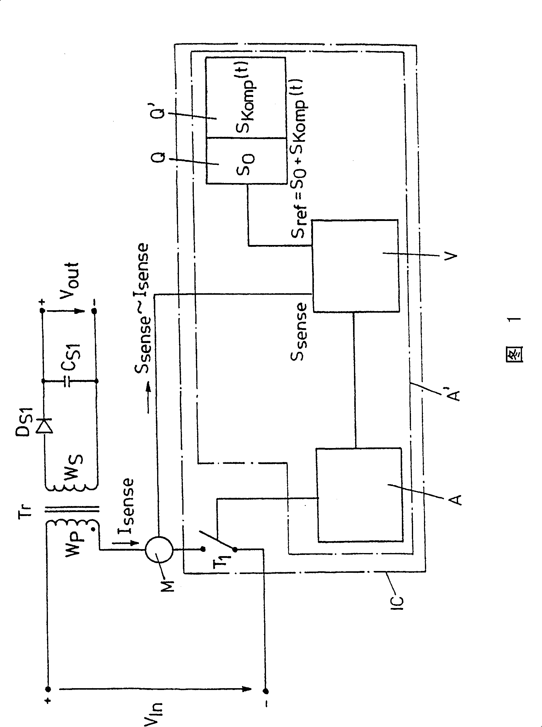
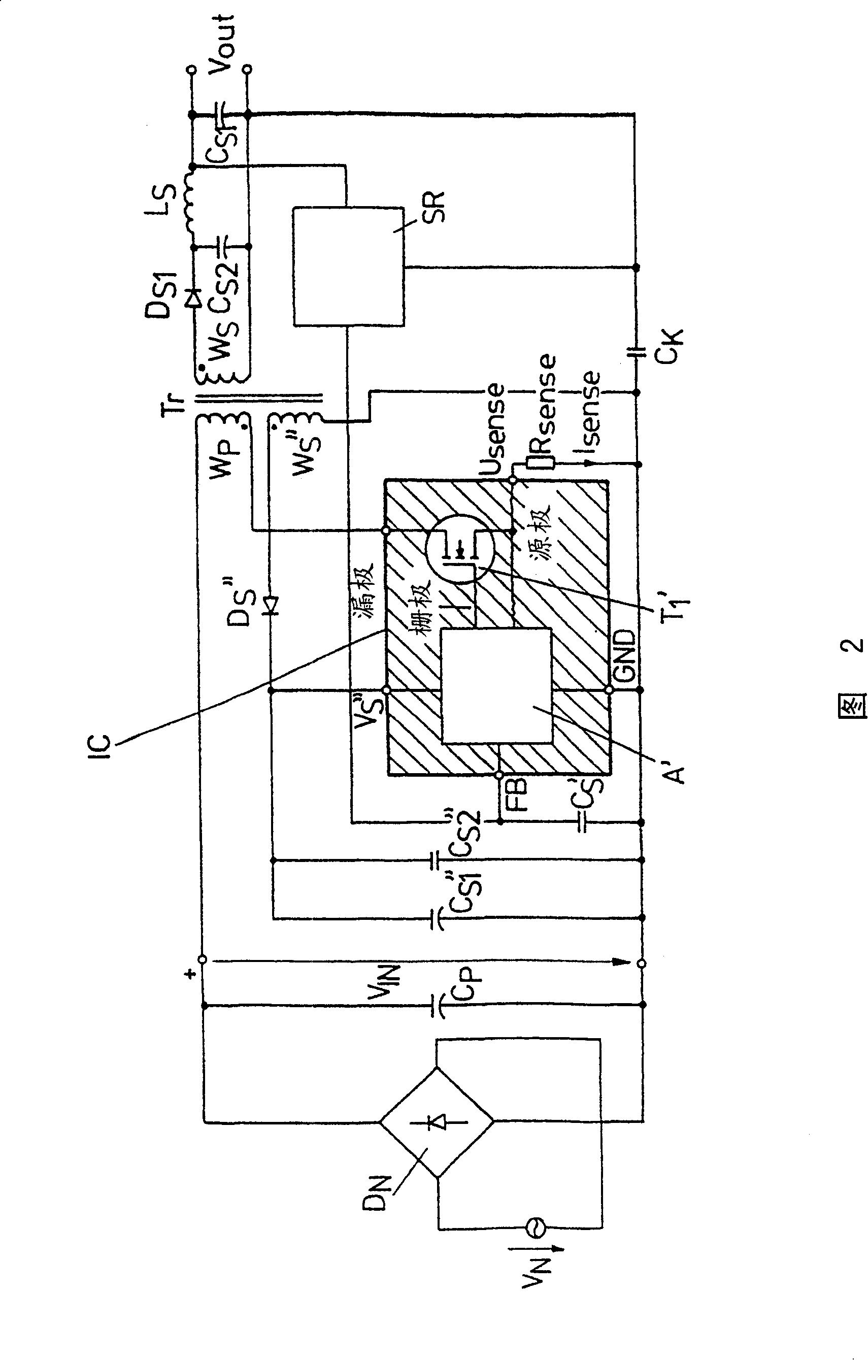
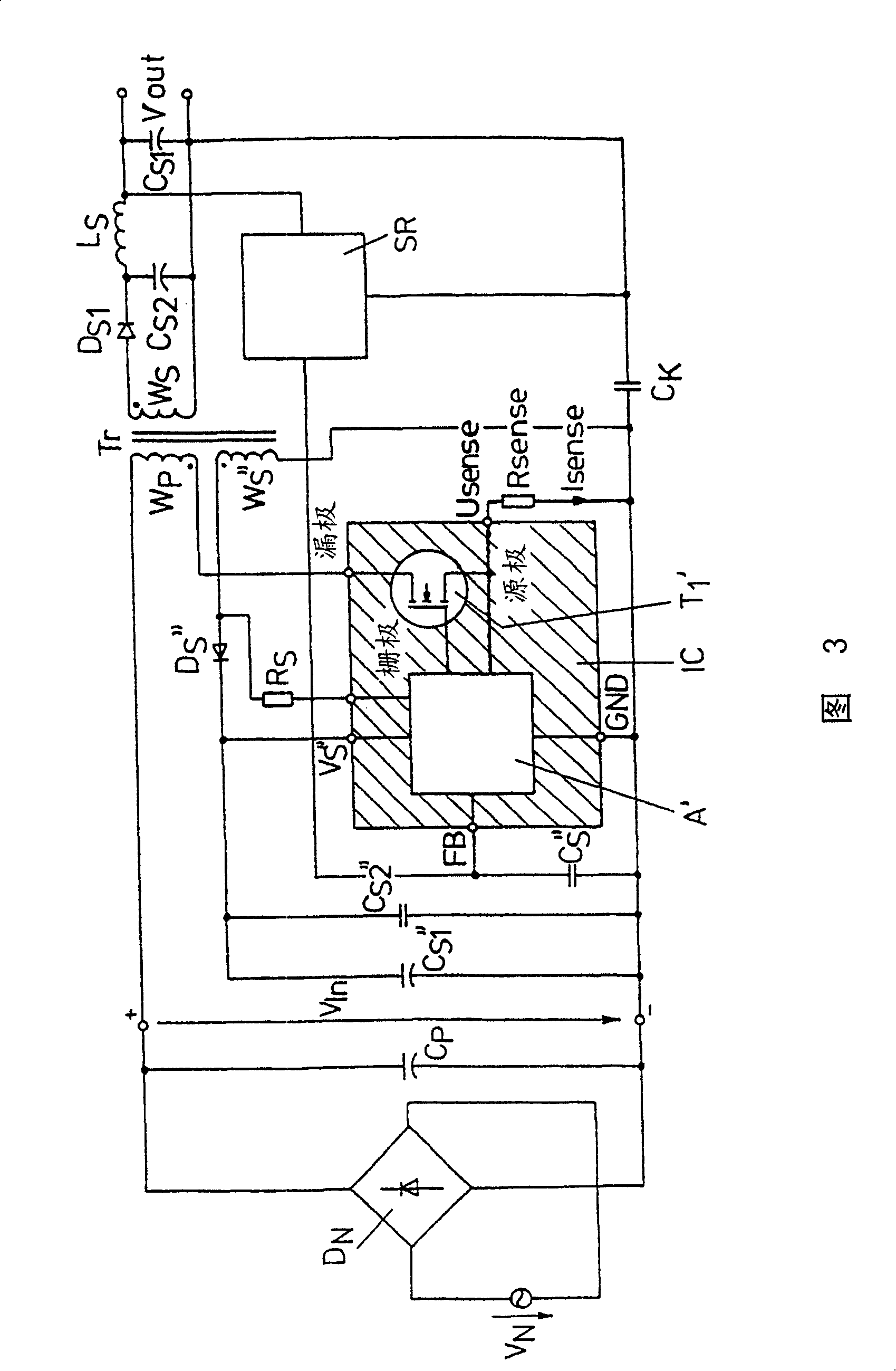
[0068] FIG. 1 shows a circuit for driving a switching power supply device according to the present invention. In this example, the switching mode power supply device is a single-ended flyback converter.
[0069] This simple flyback converter consists of a primary winding w p and a secondary winding w s The transformer Tr. A clock controls the power switch T 1 with primary winding w p in series. Input DC voltage V In Applied to the "+" and "-" terminals of this primary circuit. Input DC voltage V In Values typically range from a few volts to 400 volts.
[0070] Secondary winding w s followed by a (rectifier) diode D s1 and charge storage or smoothing capacitor C s1 . Compensation voltage V out Can be drawn on the corresponding terminal.
[0071] Switching signals are typically generated using two blocks: a pulse width modulator and a regulator with a voltage reference. The calculation method and the circuit system are described, for example, in U. Tietze and ...
PUM
 Abstract
Description
Claims
Application Information
 - R&D
- Intellectual Property
- Life Sciences
- Materials
- Tech Scout
- Unparalleled Data Quality
- Higher Quality Content
- 60% Fewer Hallucinations
Browse by: Latest US Patents, China's latest patents, Technical Efficacy Thesaurus, Application Domain, Technology Topic, Popular Technical Reports.
© 2025 PatSnap. All rights reserved.Legal|Privacy policy|Modern Slavery Act Transparency Statement|Sitemap|About US| Contact US: help@patsnap.com