Structure of package using coupling and its forming method
A packaging structure and bump technology, applied in the direction of electrical components, electrical solid devices, circuits, etc., can solve problems such as chip cracking, uneven joint surface, open circuit, etc.
- Summary
- Abstract
- Description
- Claims
- Application Information
AI Technical Summary
Problems solved by technology
Method used
Image
Examples
Embodiment Construction
[0022] A preferred embodiment of the package structure and its forming method of the present invention is described in detail as follows.
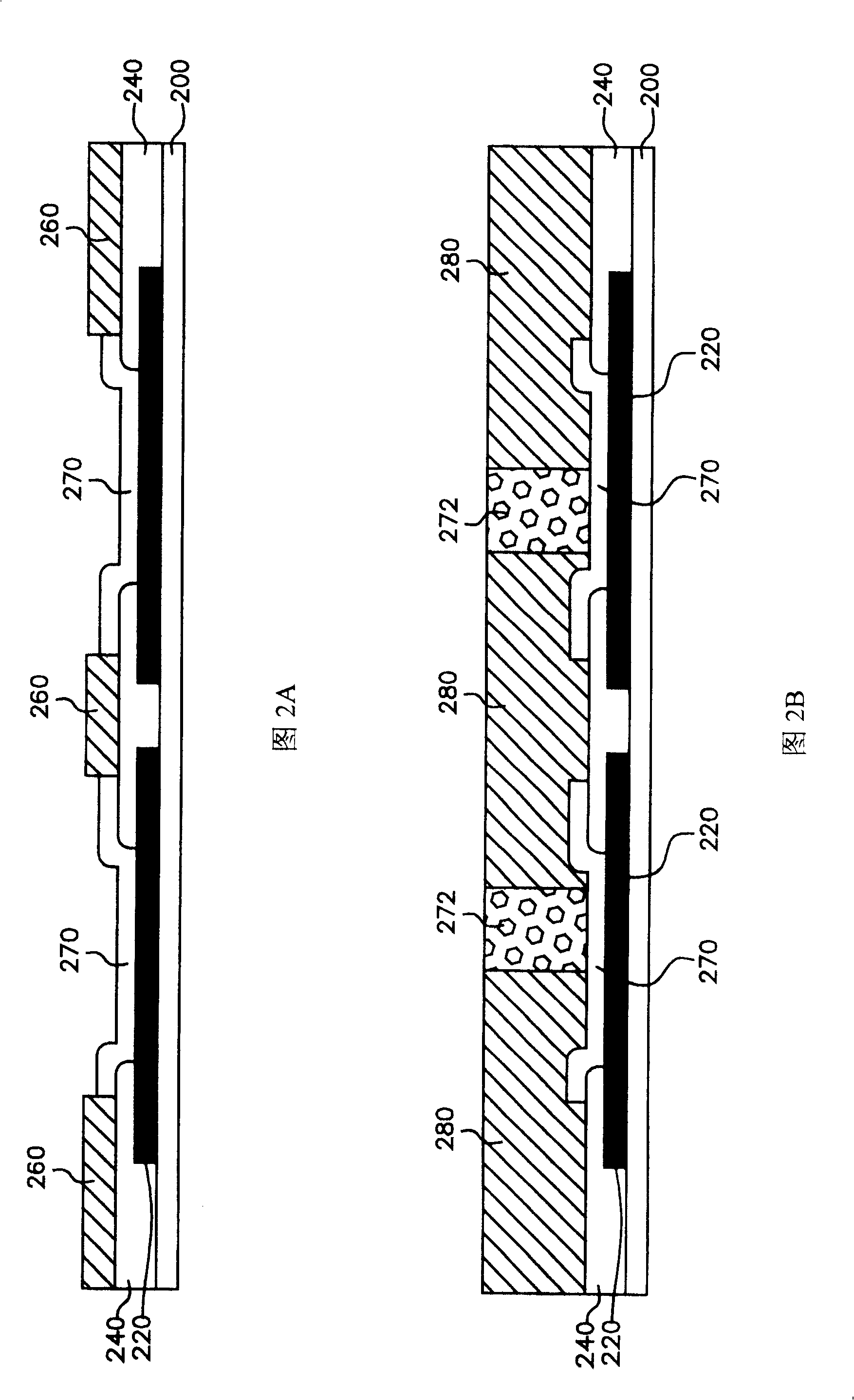
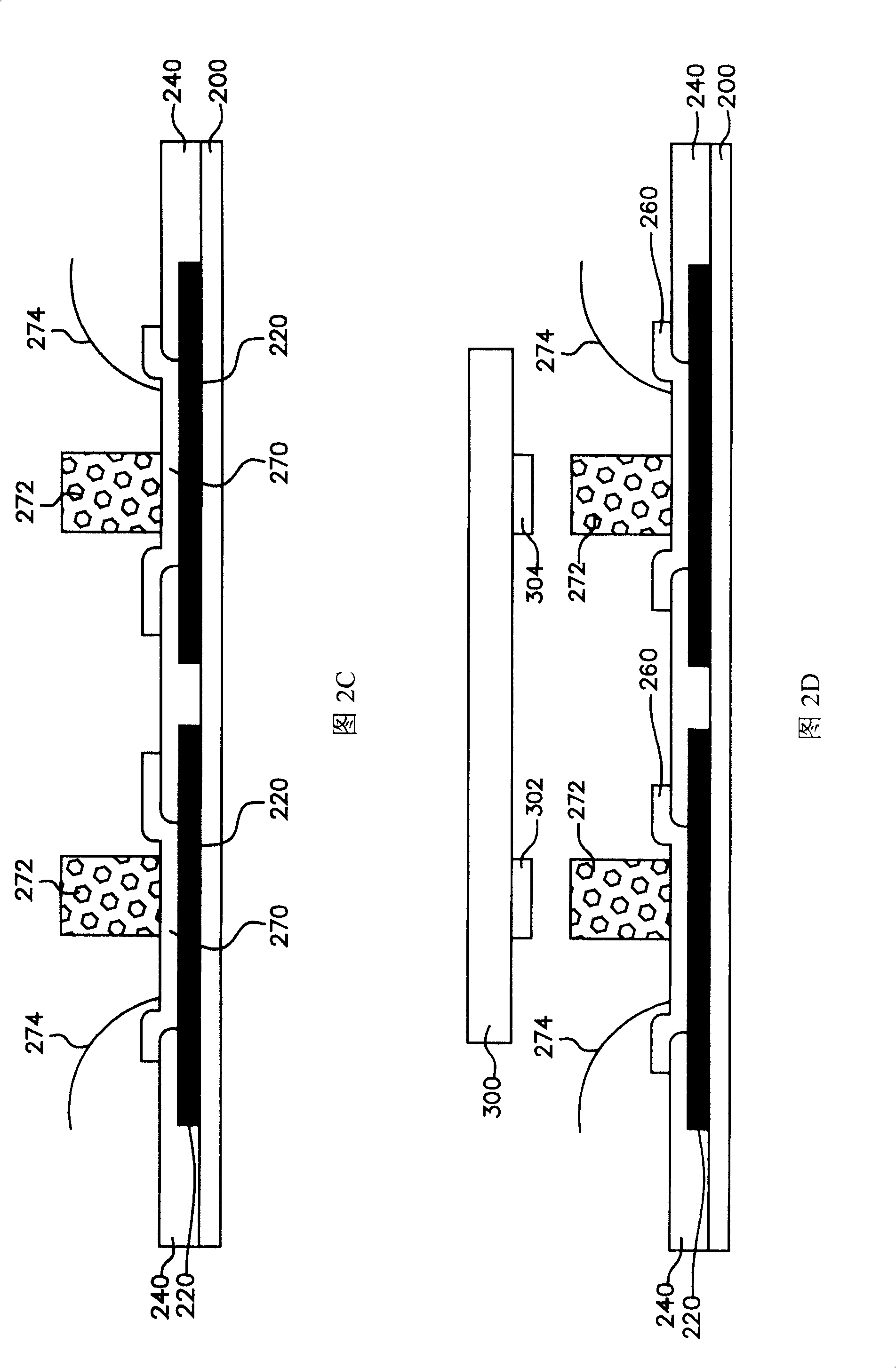
[0023] 2A to 2D are schematic cross-sectional views of the forming process of the packaging structure of the present invention. First, please refer to FIG. 2A , a pad 220 and a protective layer 240 are sequentially formed on a substrate 200 , and the protective layer 240 is formed around the pad 220 to protect components on the substrate 200 . Wherein, the material forming the pad 220 is metal, preferably an aluminum pad. Next, a mask layer 260 is formed on the protective layer 240 by using a lithography process, and the contact pad 220 is exposed to define the formation position of the first bump 270, and then an electroplating process is performed to form the first bump 270 in the defined position. A first bump 270 with a height of about 2-3 μm. The first bump 270 will completely cover the pad 220 for protecting the pad 220 as well as ...
PUM
 Abstract
Description
Claims
Application Information
 - R&D
- Intellectual Property
- Life Sciences
- Materials
- Tech Scout
- Unparalleled Data Quality
- Higher Quality Content
- 60% Fewer Hallucinations
Browse by: Latest US Patents, China's latest patents, Technical Efficacy Thesaurus, Application Domain, Technology Topic, Popular Technical Reports.
© 2025 PatSnap. All rights reserved.Legal|Privacy policy|Modern Slavery Act Transparency Statement|Sitemap|About US| Contact US: help@patsnap.com


