Structure of package using coupling and its forming method

A packaging structure and bump technology, applied in the direction of electrical components, electrical solid devices, circuits, etc., can solve the problems of lower product yield, open circuit, contact short circuit, etc.

Active Publication Date: 2006-10-04
CHIPMOS TECH INC
View PDF0 Cites 2 Cited by
  • Summary
  • Abstract
  • Description
  • Claims
  • Application Information

AI Technical Summary

Problems solved by technology

[0006] When the two bumps are joined, the uneven contact surface can easily lead to poor joint quality, resulting in short circuit or open circuit of the contact
And this uneven surface, when bonding the substrate and the chip, is easy to cause the crack of the chip, reducing the product yield, and the larger the chip to be bonded, the more uneven the joint surface will be. tricky

Method used


Image

  • Structure of package using coupling and its forming method
  • Structure of package using coupling and its forming method
  • Structure of package using coupling and its forming method

Examples


Embodiment Construction

[0022] A preferred embodiment of the package structure and its forming method of the present invention is described in detail as follows.

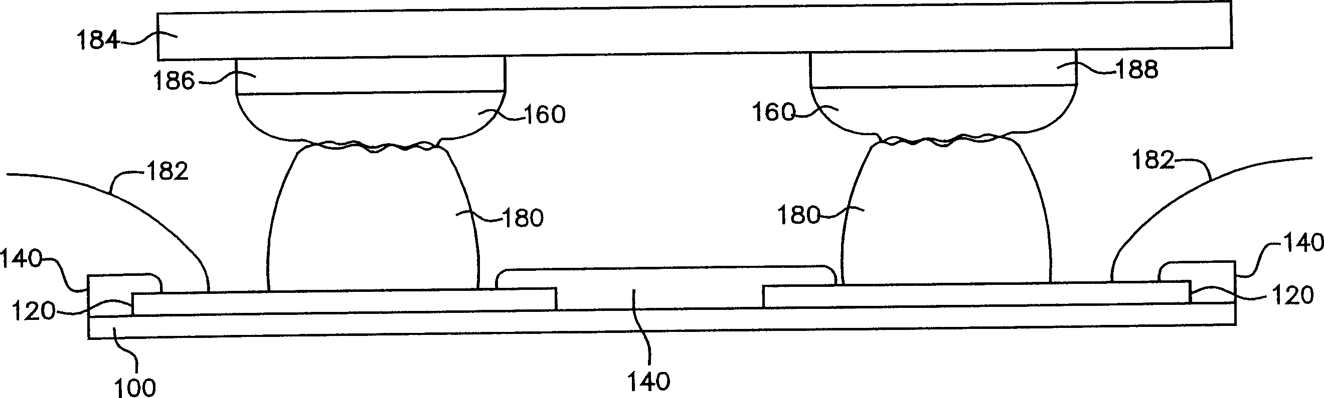
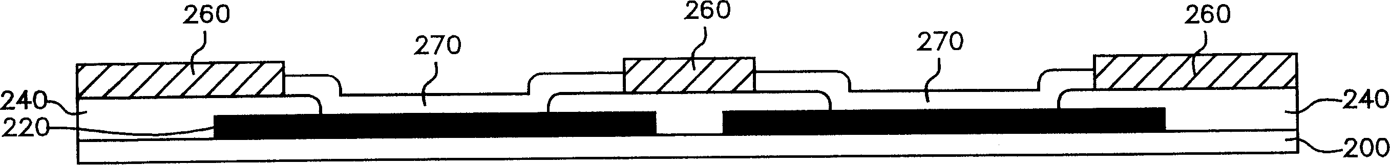
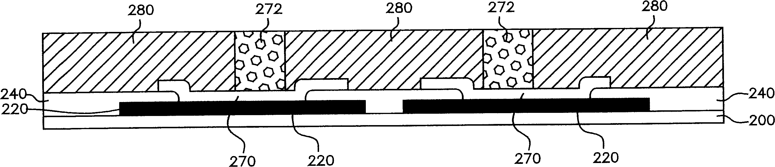
[0023] Figures 2A to 2D It is a schematic cross-sectional view of the forming process of the packaging structure of the present invention. First please refer to Figure 2A , sequentially forming a pad 220 and a protection layer 240 on a substrate 200 , the protection layer 240 is formed around the pad 220 to protect components on the substrate 200 . Wherein, the material forming the pad 220 is metal, preferably an aluminum pad. Next, a mask layer 260 is formed on the protective layer 240 by using a lithography process, and the contact pad 220 is exposed to define the formation position of the first bump 270, and then an electroplating process is performed to form the first bump 270 in the defined position. A first bump 270 with a height of about 2-3 μm. The first bump 270 will completely cover the pad 220 for protecting the pad 220 as...


PUM


Abstract

The invention relates to a structure for using projection to seal and it's forming method. It first forms a barrier and an adhesion coating layer on a base material with a pad and a protecting layer, and then it forms a first projection and a second projection on the flat region of the first projection and at lest connects the external electrode of the chip on the second projection.

Description

technical field [0001] The present invention relates to a packaging structure, and in particular to a flip-chip packaging structure. Background technique [0002] A light-emitting diode is a light-emitting component that can directly convert electrical energy into visible light. It has the characteristics of low operating voltage, low power consumption, and high luminous efficiency. The core light-emitting part of the light-emitting diode is composed of P-type and N-type semiconductors. When the minority carrier injected into the PN junction recombines with the majority carrier, it will emit visible light, ultraviolet light or near-infrared light. [0003] For GaN series high-brightness light-emitting diodes using sapphire substrates, since the PN electrodes are located below, flip-chip packaging can provide 1.5 to 1.7 times the luminous efficiency compared with wire-bonding packaging due to the non-shielding characteristics. Moreover, the heat energy generated by the light...

Claims


Application Information

Patent Timeline
Patent Type & Authority Applications(China)
IPC IPC(8): H01L33/00H01L23/48H01L21/60H01L33/62
CPCH01L24/81H01L24/11H01L2224/11H01L2924/00012
Inventor 王俊恒
Owner CHIPMOS TECH INC
Why Eureka
Try Eureka