
Flexible display substrate, display panel, display device and manufacturing method

A flexible display and manufacturing method technology, applied in the directions of identification devices, final product manufacturing, climate sustainability, etc., can solve the problems of flexible display substrates such as subsidence, breakage, or contact with driver ICs, product short circuits, etc., to improve the binding process Yield rate, weaken further deformation, effect of guarantee binding effect

Active Publication Date: 2021-08-06
BOE TECH GRP CO LTD +1
View PDF11 Cites 0 Cited by
  • Summary
  • Abstract
  • Description
  • Claims
  • Application Information

AI Technical Summary

Problems solved by technology

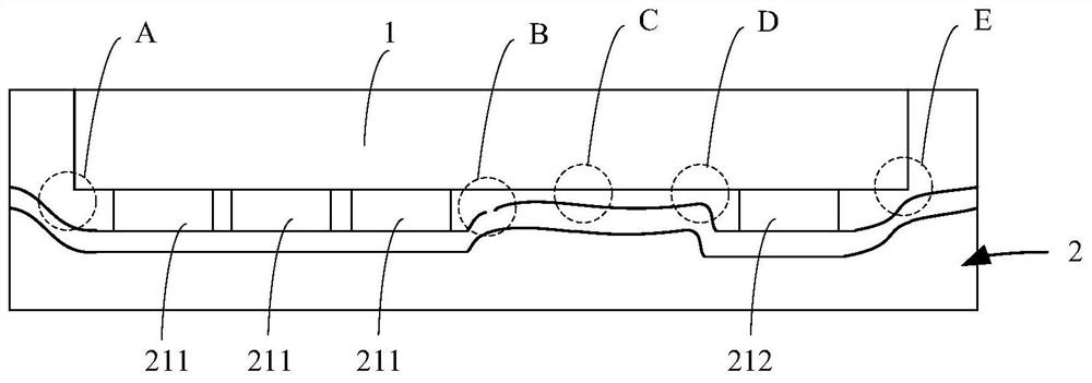
[0004] Since the binding area on the flexible display substrate is more prominent than the non-binding area, during the binding process, the binding area will first be squeezed by the bump of the driver IC. The extrusion of the bumps of the driver IC will easily cause the area around the binding area of ​​the flexible display substrate to sag, causing deformation of the flexible display substrate. When the deformation of the flexible display substrate is too large, the metal wiring on the flexible display substrate may be broken or damaged. In contact with the driver IC, the breakage of the metal wiring will cause an open circuit problem in the product, and the contact of the metal wiring with the driver IC will cause a short circuit problem in the product

Method used


Image

  • Flexible display substrate, display panel, display device and manufacturing method
  • Flexible display substrate, display panel, display device and manufacturing method
  • Flexible display substrate, display panel, display device and manufacturing method

Examples


Embodiment Construction

[0045] In order to make the object, technical solution and advantages of the present invention clearer, the implementation manner of the present invention will be further described in detail below in conjunction with the accompanying drawings.

[0046] Increasing the screen-to-body ratio (that is, the area ratio of the display screen in the display device) is a development trend of OLED display devices at present. At present, an effective way to increase the screen ratio is to bind the driver chip on the flexible display substrate through the COP process. The COP process makes full use of the foldability of the flexible display substrate, and folds the part of the flexible display substrate with the driver chip to the back of the display screen, thereby increasing the screen-to-body ratio. However, since the rigidity of the flexible display substrate is not high, it is prone to deformation during the binding process, resulting in defective defects of the display device.

[00...


PUM


Abstract

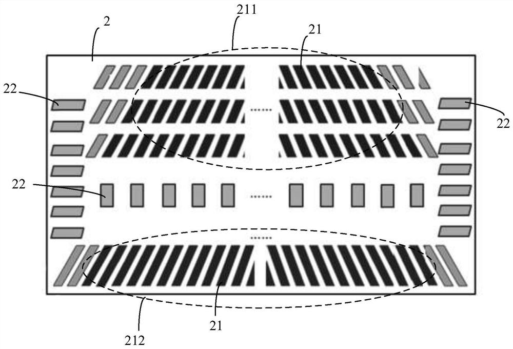
The invention discloses a flexible display substrate, a display panel, a display device and a manufacturing method, and belongs to the field of display technology. The flexible display substrate has a first binding area and a second binding area, the first binding area is used for binding with electronic components for signal transmission with the electronic components, and the second binding area For binding with electronic components but without signal transmission, in a direction perpendicular to the flexible display substrate, the thickness of the flexible display substrate at the first binding region is greater than that of the flexible display substrate at the The thickness of the second binding region. The invention can reduce the warping deformation of the flexible display substrate during the binding process with the electronic components, and improve the yield rate of the binding process.

Description

technical field [0001] The invention relates to the field of display technology, in particular to a flexible display substrate, a display panel, a display device and a manufacturing method. Background technique [0002] Flexible display substrates are more and more widely used in (Organic Light-Emitting Diode, OLED) display devices due to their thinness and good impact resistance. An OLED display device generally includes a flexible display substrate and a driver integrated circuit (Driver Integrated Circuit, Driver IC), and the driver IC is bound on the flexible display substrate. [0003] At present, the binding methods of driver ICs mainly include COF (Chip On Film) and COP (Chip On Plastic). In the COP binding method, after the driver IC is bound to the flexible display substrate, the part of the flexible display substrate with the driver IC can be folded to the back of the flexible display substrate, so that the area of ​​the display area of ​​the flexible display subs...

Claims


Application Information

Patent Timeline
Patent Type & Authority Patents(China)
IPC IPC(8): G09F9/30H01L27/32H01L51/00H01L51/52H01L51/56H10K99/00
CPCG09F9/30Y02E10/549H01L27/124H01L27/1218Y02P70/50H10K59/1213H10K59/131H10K77/111H10K50/8426H10K50/844H10K71/00H10K2102/311
Inventor 周宏军梁恒镇
Owner BOE TECH GRP CO LTD
Learn More