Electro-optical device, method of driving electro-optical device, and electronic apparatus
An electro-optical device and driving circuit technology, applied in optics, nonlinear optics, instruments, etc., can solve problems such as picture quality degradation, and achieve the effects of reducing circuit scale, power consumption, and power consumption.
- Summary
- Abstract
- Description
- Claims
- Application Information
AI Technical Summary
Problems solved by technology
Method used
Image
Examples
no. 1 Embodiment approach
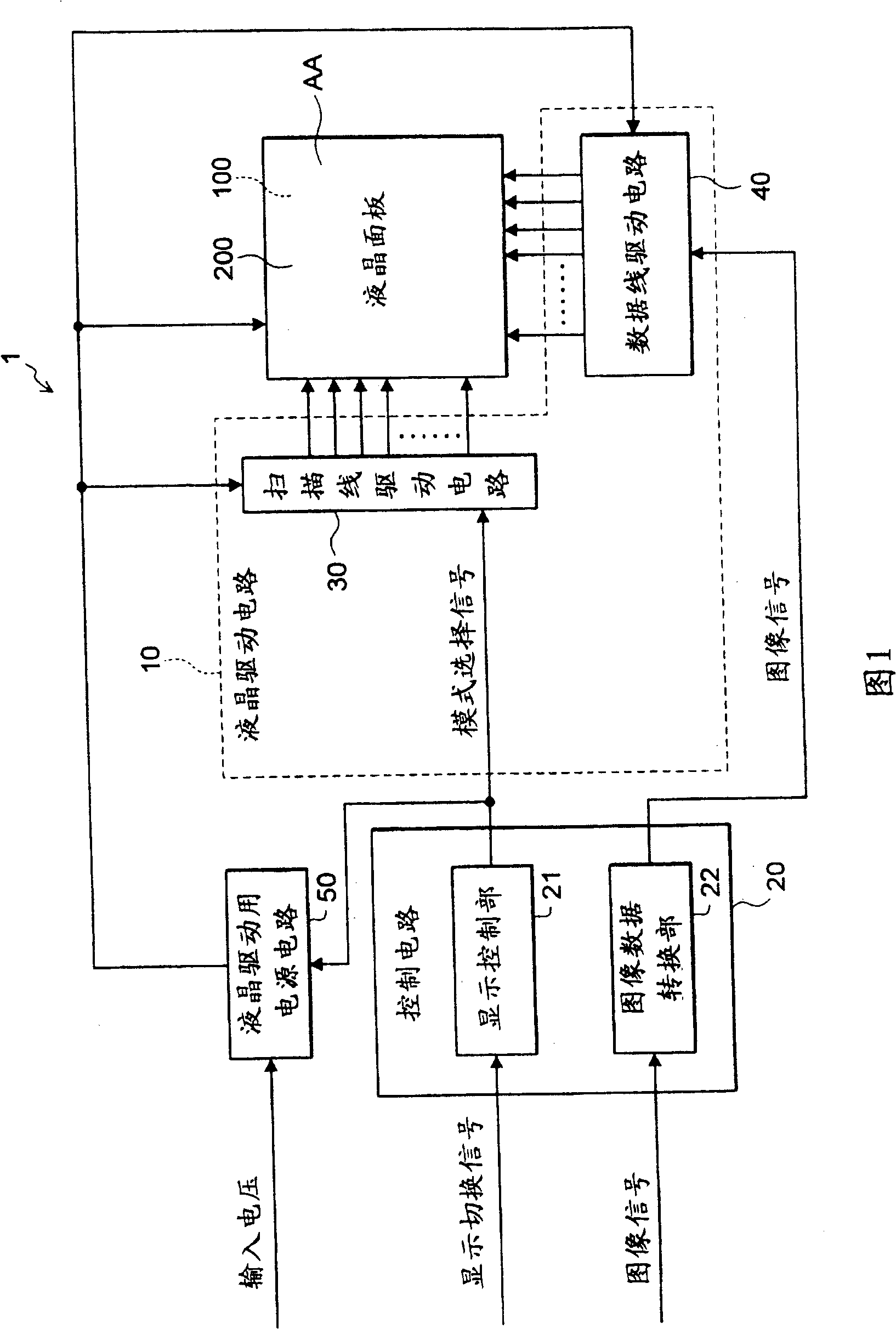
[0055] FIG. 1 is a block diagram of an electro-optical device 1 according to a first embodiment of the present invention.
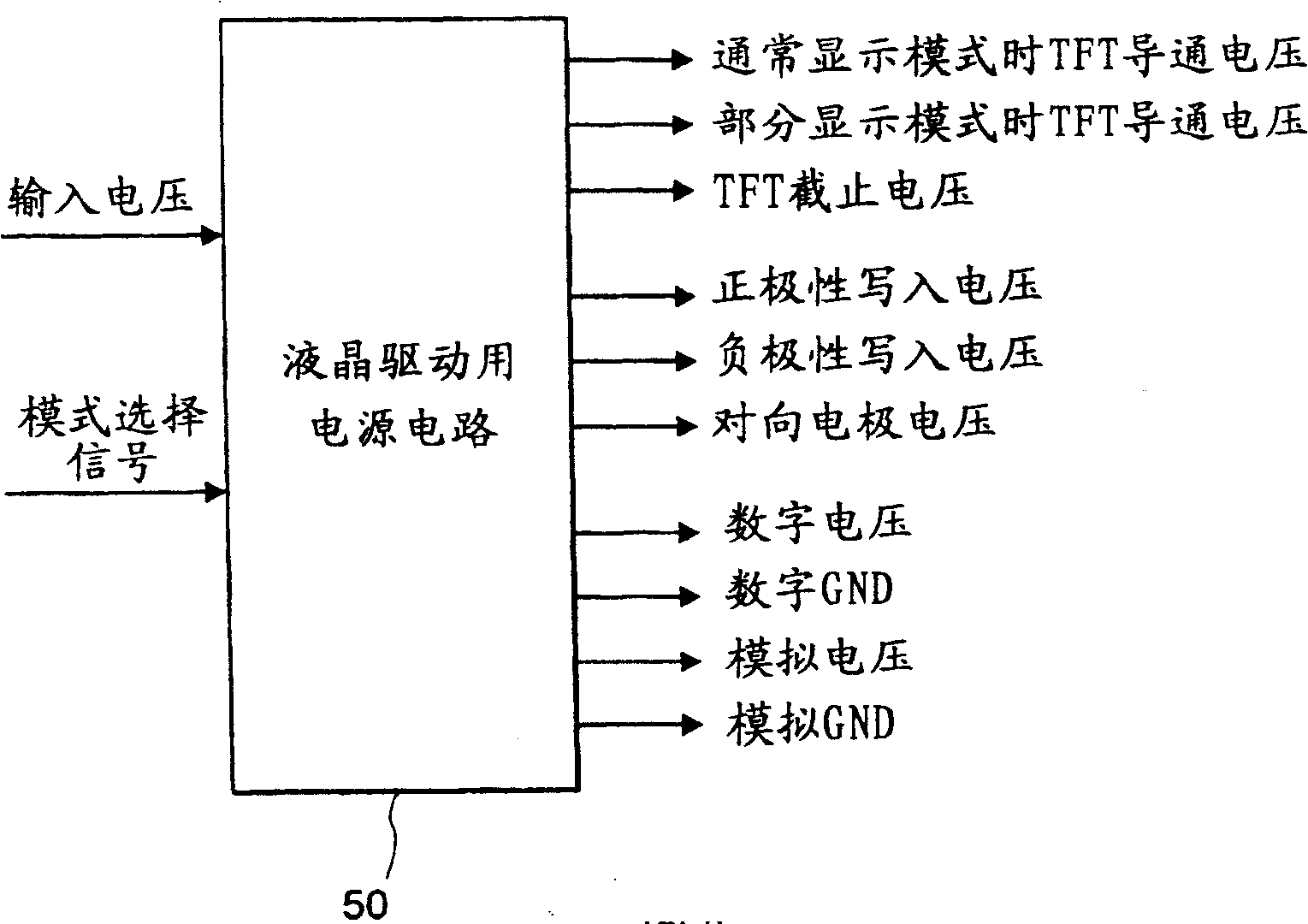
[0056] The electro-optical device 1 has: a liquid crystal panel AA; a liquid crystal driving circuit 10, which is used to drive the liquid crystal panel AA; a control circuit 20, which is used to control the liquid crystal driving circuit 10; and a liquid crystal driving power supply circuit 50, which is used to supply the liquid crystal panel AA and The liquid crystal drive circuit 10 supplies voltage. The liquid crystal drive circuit 10 includes a scan line drive circuit 30 and a data line drive circuit 40 . The control circuit 20 includes a display control unit 21 and an image data conversion unit 22 .
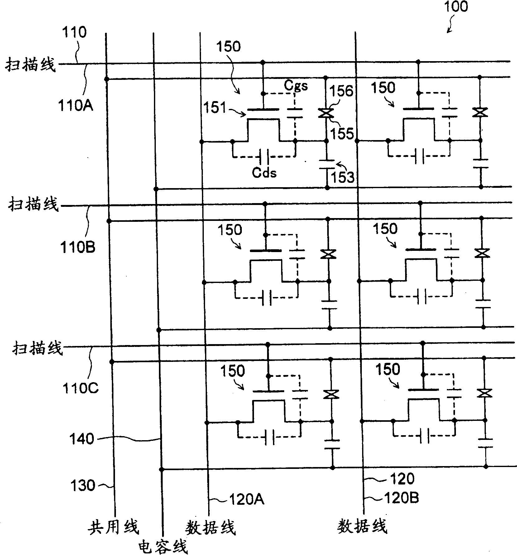
[0057] figure 2 It is a partial enlarged plan view of liquid crystal panel AA.
[0058] The liquid crystal panel AA includes (see FIG. 1 ): an element substrate 100 as a first substrate in which thin film transistors (hereinafter referred to as TFTs...
no. 2 Embodiment approach
[0111] Figure 7 is a circuit diagram of the charge pump circuit 51 according to the second embodiment of the present invention. The charge pump circuit 51 is provided in the power supply circuit 50 for driving liquid crystal, and includes a first charge pump unit circuit 511 and a second charge pump unit circuit 512 .
[0112] The first charge pump unit circuit 511 includes input terminals A and B and an output terminal C. As shown in FIG. The first charge pump unit circuit 511 adds the potential difference between the input terminals A and B to the voltage at the input terminal A, and outputs it from the output terminal C. That is, the first charge pump unit circuit 511 approximately doubles the voltage at the input terminal A, and outputs it from the output terminal C.
[0113] Specifically, the first charge pump unit circuit 511 includes: a capacitor 511A; a switching element 511B for connecting one end of the capacitor 511A to the input terminal A or output terminal C; ...
no. 3 Embodiment approach
[0127] FIG. 8 is a circuit diagram of a charge pump circuit 52 according to a third embodiment of the present invention. and Figure 7 The difference of the charge pump circuit 51 is the value of the digital voltage that boosts the digital input voltage and outputs it. The charge pump circuit 52 is provided in the liquid crystal drive power supply circuit, and includes a third charge pump unit circuit 521 , a fourth charge pump unit circuit 522 , and a fifth charge pump unit circuit 523 .
[0128] The third charge pump unit circuit 521 has input terminals P and Q and an output terminal R. FIG. The third charge pump unit circuit 521 is used to add the potential difference between the input terminals P and Q to the voltage of the input terminal P, and output it from the output terminal R. That is, the third charge pump unit circuit 521 substantially doubles the voltage at the input terminal, and outputs it from the output terminal R.
[0129] Specifically, the third charge pu...
PUM
 Abstract
Description
Claims
Application Information


