Decoupling reactive ion etching chamber containing multiple processing platforms

A processing chamber and etching chamber technology, applied in the field of plasma processing chambers, can solve the problems of not being able to ensure strict performance specifications, increasing the complexity of the structure and configuration of the processing chamber, etc.

Active Publication Date: 2009-01-14
ADVANCED MICRO FAB EQUIP INC CHINA
View PDF14 Cites 1 Cited by
  • Summary
  • Abstract
  • Description
  • Claims
  • Application Information

AI Technical Summary

Problems solved by technology

In particular, the '681 patent explains that the inadequacy of the Mattson system (the subject of the aforementioned '022 patent) is limited by the localized processing of multiple substrates in multiple stations within a single chamber. directly caused by
This increases the complexity of the structure and configuration of the processing chamber
Finally, the aforementioned methods of generating plasma in parallel processing chambers do not ensure meeting the stringent performance specifications required for the fabrication of advanced semiconductor devices

Method used


Image

  • Decoupling reactive ion etching chamber containing multiple processing platforms
  • Decoupling reactive ion etching chamber containing multiple processing platforms
  • Decoupling reactive ion etching chamber containing multiple processing platforms

Examples


Embodiment Construction

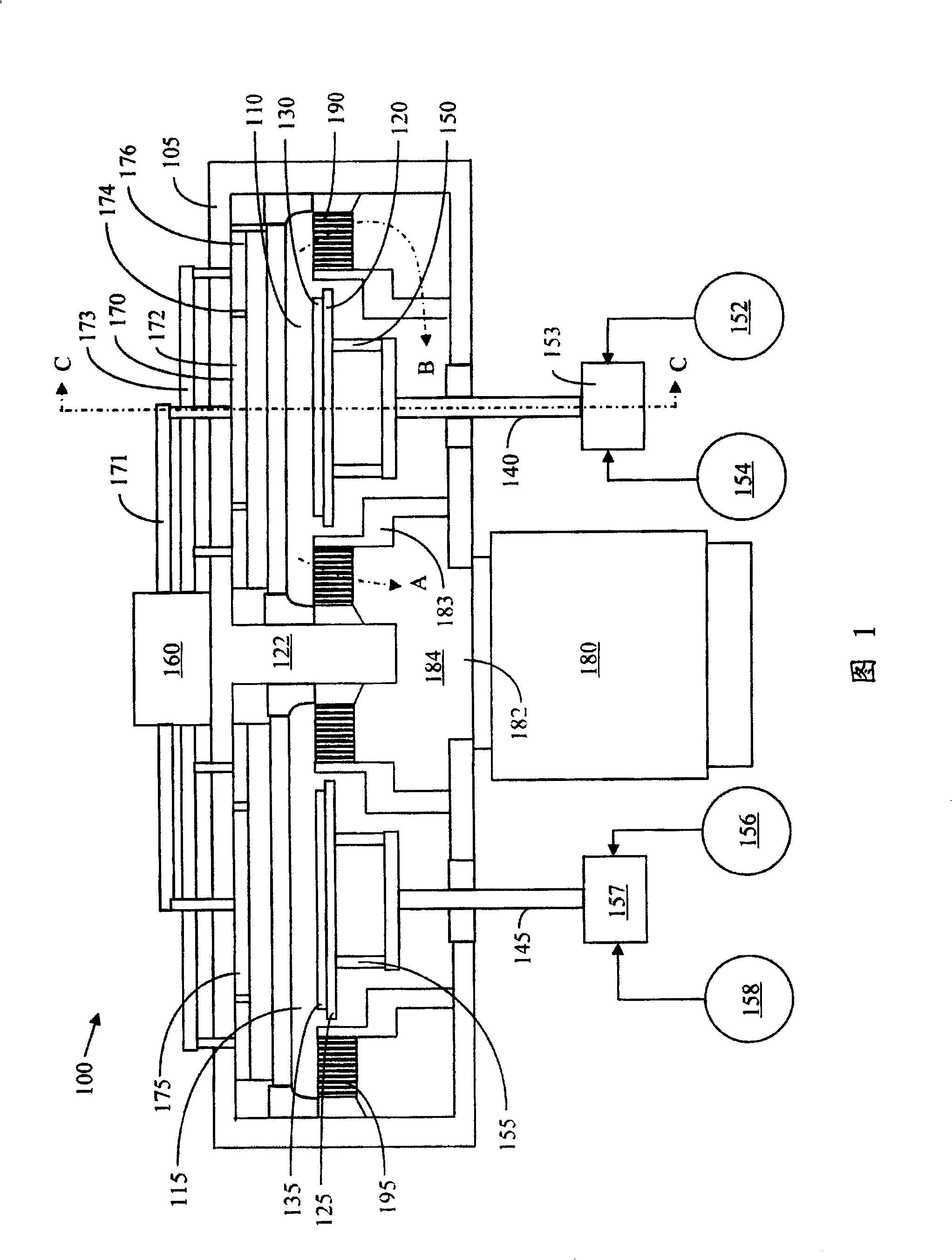
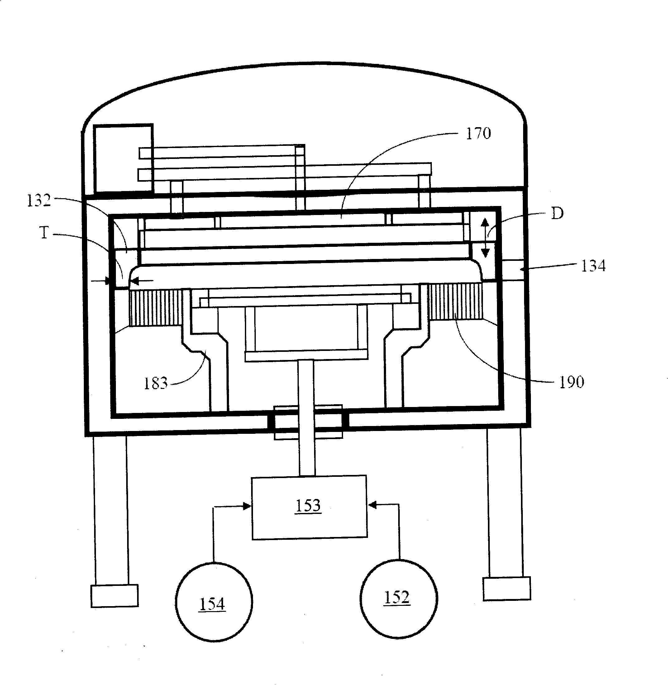
[0023] Embodiments of the present invention provide a versatile plasma chamber that can provide high precision uniformity processing at high throughput. The invention can realize the stability and consistency of the plasma in each processing area, and the obtained processing results meet the high-precision requirements in advanced semiconductor processing. The present invention provides a multi-station decoupled reactive ion etch chamber having multiple processing platforms or processing regions, wherein each processing region is applied with multiple RF power sources. The present invention adopts various characteristics and designs to prevent frequency fluctuation and radio frequency crosstalk between two adjacent parallel processing areas. In particular, to date no one has proposed feeding two or more RF frequencies to the cathodes of each processing zone in parallel processing chambers to achieve decoupled reactive ion etching.

[0024] 1 is a cross-sectional view of a par...


PUM


Abstract

The invention is used for isolating the plasma and RF. In the invention, each handling area at least has two RF frequencies feeding in its cathode; wherein, one RF frequency is at least two times higher than the other one so as to provide the decoupling reactive ion etching capability; the room body of the handling room is grounded. By the frequency isolation, the multi RF frequencies fed-in from cathode is not able to bring RF cross talk and fluctuation. The invention also uses a plasma restraint device to avoid the cross talk of plasma. A grounded shared exhaust passage is attached to the vacuum pump.

Description

【Technical field】 [0001] The present invention relates to a plasma processing chamber, in particular to a plasma processing chamber with one pair or more parallel processing regions, which can process two or more substrates individually or simultaneously. 【Background technique】 [0002] During the fabrication of semiconductor chips, two types of semiconductor chip processing systems are generally used. The first type of system is often referred to as a batch processing (batch processing) system. The main reason for using a batch system is that multiple chips or substrates can be processed simultaneously, thus the system can provide high output throughput. However, as semiconductor device performance specifications have become increasingly stringent, the industry has turned to a second type of chamber, ie, a single substrate chamber. The main reason for developing a single substrate processing system is that it is easier to control the process characteristics of the substra...

Claims


Application Information

Patent Timeline
Patent Type & Authority Patents(China)
IPC IPC(8): H05H1/46H01L21/00H01L21/67H01J37/32
CPCH01J37/3211H01J37/32165H01J37/32183H01J37/32623H01J37/32899H01L21/67069
Inventor 尹志尧倪图强陈金元钱学煜
Owner ADVANCED MICRO FAB EQUIP INC CHINA
Why Eureka
Try Eureka