Nand flash memory device and method of forming a well of a nand flash memory device

A flash memory, storage unit technology, applied in information storage, static memory, read-only memory, etc., can solve problems such as failure to achieve target device indicators, failure to save data status, and erasure interference.

Inactive Publication Date: 2009-03-04
SK HYNIX INC
View PDF3 Cites 0 Cited by
  • Summary
  • Abstract
  • Description
  • Claims
  • Application Information

AI Technical Summary

Problems solved by technology

Therefore, there will be a problem that the state of the data cannot be saved due to the phenomenon of shallow erasure
In addition, due to the erasure interference, there is a problem that the target device cannot be achieved.

Method used


Image

  • Nand flash memory device and method of forming a well of a nand flash memory device
  • Nand flash memory device and method of forming a well of a nand flash memory device
  • Nand flash memory device and method of forming a well of a nand flash memory device

Examples


Embodiment Construction

[0014] Preferred embodiments according to the present invention will now be described with reference to the accompanying drawings. Since the preferred embodiments are provided to enable those skilled in the art to understand the present invention, the preferred embodiments can be modified in various ways and the scope of the present invention is not limited to the preferred embodiments described later. Also, in the drawings, the same reference symbols are used to designate the same or similar components.

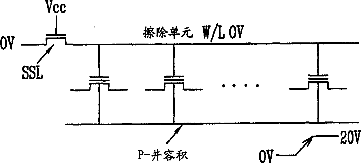
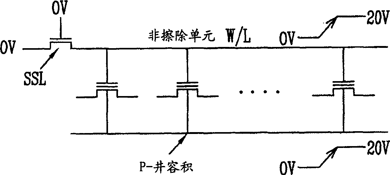
[0015] Figure 2A and Figure 2B is shown to illustrate an overview of a NAND flash memory device according to the present invention.

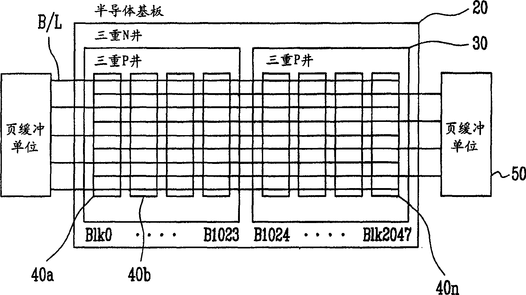
[0016] refer to Figure 2A and Figure 2B , according to a specific embodiment of the present invention, the NAND flash memory device may include a triple N well 20 formed in the semiconductor substrate to electrically protect a plurality of memory cells in a specific area of ​​the semiconductor substrate; two or more A triple P well 30...


PUM


Abstract

Disclosed herein are a NAND flash memory device and a method of forming a well of the NAND flash memory device. Triple wells of a NAND flash memory device are formed within a cell region in plural. A cell block including flash memory cells is formed on the triple wells. Accordingly, during an erase operation of a flash memory device, a stress time for non-selected blocks can be reduced and erase disturbance can be also prevented, through the plurality of the wells. Further, capacitance between the triple P wells and the triple N well is reduced since triple P wells are divided. Therefore, well bias charging and discharging time can be reduced and an overall erase time budget can be thus reduced.

Description

technical field [0001] The present invention relates to a NAND (NAND) flash memory device and a method of forming a well of the NAND flash memory device, and more particularly, to a well formed in a cell region of the NAND flash memory device. Background technique [0002] Generally, in NAND flash memory devices, cells are erased by F-N tunneling. The NAND flash memory cell is formed on a single P-well. A plurality of units are formed into a ribbon to form a unit string. Multiple unit strings are arranged vertically or horizontally to form a unit block. Therefore, an erase operation is performed by the block of cells. [0003] Figure 1A and Figure 1B An overview diagram is shown to illustrate a conventional erase operation. [0004] refer to Figure 1A and Figure 1B , a 0V voltage is applied to the word line W / L of the selected cell block through the string selection transistor SSL. The word lines W / L of the unselected cell blocks are floated via the string selecti...

Claims


Application Information

Patent Timeline
Patent Type & Authority Patents(China)
IPC IPC(8): H01L27/10H01L27/115H01L21/76H01L21/8239H01L21/761G11C16/00G11C16/04G11C16/16H01L21/8247H01L29/76H01L29/788H01L29/792H01L29/94
CPCG11C16/0483H01L21/8239H01L27/11517G11C16/16H01L27/1052H10B99/00H10B41/00
Inventor 李熙烈
Owner SK HYNIX INC
Why Eureka
Try Eureka