Pixel unit, pixel circuit and driving method thereof

A pixel unit and pixel circuit technology, applied in static indicators, instruments, etc., can solve the problems of drive current difference, display brightness difference, threshold voltage drift, etc., to prolong service life, shorten stress time, and reduce misoperation rate Effect

Active Publication Date: 2016-08-17
BOE TECH GRP CO LTD +1
View PDF5 Cites 0 Cited by
  • Summary
  • Abstract
  • Description
  • Claims
  • Application Information

AI Technical Summary

Problems solved by technology

However, due to the limitations of the crystallization process, low-temperature polysilicon thin film transistors fabricated on large-area glass substrates often have non-uniformity in electrical parameters such as threshold voltage and mobility. This non-uniformity will translate into OLED devices. The difference in driving current and brightness is perceived by the human eye as color unevenness
Although the process uniformity of the oxide thin film transistor is good, but similar to the amorphous silicon thin film transistor, its threshold voltage will drift under long-term pressure and high temperature. Different amounts will cause differences in display brightness. Since this difference is related to the previously displayed image, it often appears as an afterimage phenomenon.

Method used


Image

  • Pixel unit, pixel circuit and driving method thereof
  • Pixel unit, pixel circuit and driving method thereof
  • Pixel unit, pixel circuit and driving method thereof

Examples


Embodiment 1

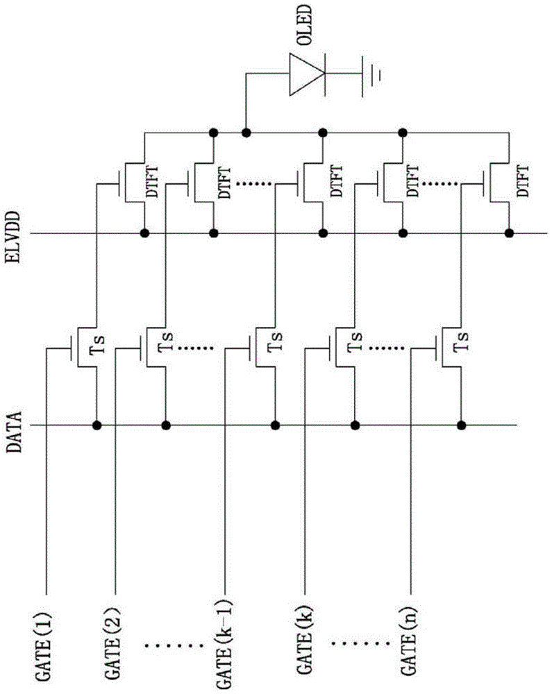
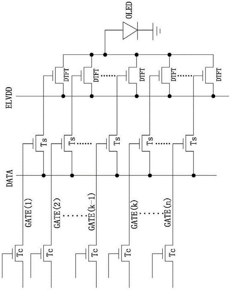
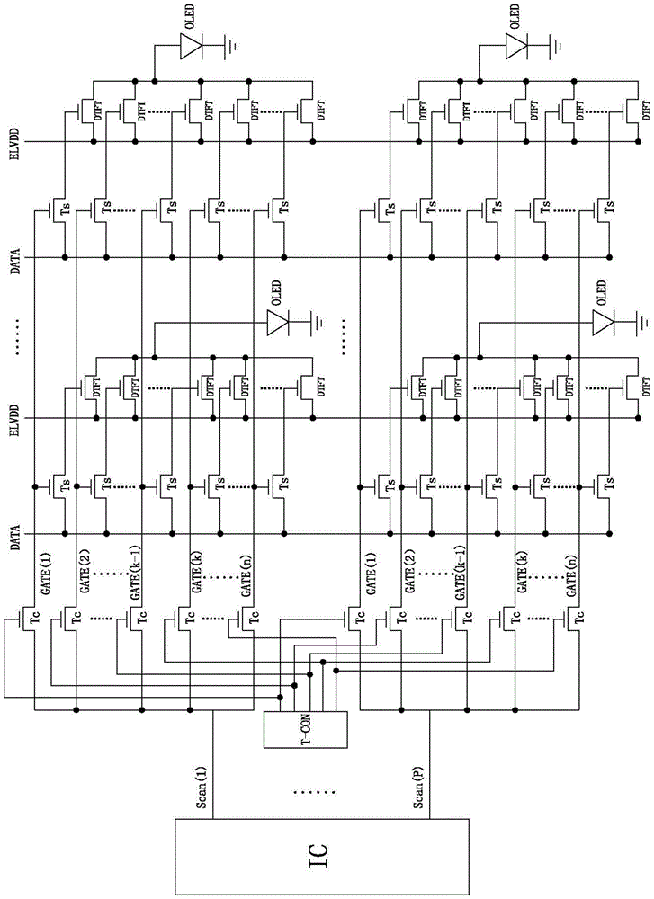
[0038] see figure 1 As shown, the pixel unit described in the embodiment of the present invention is mainly used for driving each light-emitting device in an active matrix organic light-emitting diode display, and each light-emitting device is driven by a pixel unit; each pixel unit includes a light-emitting device and n driving Sub-circuit; wherein, n is the number of driving sub-circuits, and n is a natural number, n>1;

[0039] Each of the driving sub-circuits includes a control electrode scanning signal line GATE, a switching transistor Ts and a driving transistor DTFT; the control electrode of the switching transistor is connected to the control electrode scanning signal line, the first pole is connected to the data line DATA, and the second pole is connected to the control electrode scanning signal line. connected to the control pole of the driving transistor; the first pole of the driving transistor is connected to the power supply line ELVDD, and the second pole is con...


PUM


Abstract

The present invention relates to the field of display technology, in particular to a pixel unit and a pixel circuit including the pixel unit and a driving method thereof; it includes a light-emitting device and n driving sub-circuits; wherein, n is a natural number and n>1; The driving sub-circuits all include a control electrode scanning signal line, a switch transistor and a driving transistor; the control electrode of the switching transistor is connected to the control electrode scanning signal line, the first electrode is connected to the data line, and the second electrode is connected to the control electrode of the driving transistor; The first electrode of the driving transistor is connected to the power supply line, the second electrode is connected to the third electrode of the light-emitting device; the fourth electrode of the light-emitting device is connected to the reference voltage terminal. The present invention adopts the design of n (n>1) driving sub-circuits for driving the light-emitting device to emit light; each driving sub-circuit can drive the light-emitting device to emit light according to the time sequence; this form can effectively shorten the time in each driving sub-circuit Stress time of the drive transistor.

Description

technical field [0001] The present invention relates to the field of display technology, in particular to a pixel unit, a pixel circuit including the pixel unit and a driving method thereof. Background technique [0002] Organic Light-Emitting Diode (OLED, Organic Light-Emitting Diode), as a current-mode light-emitting device, has been increasingly used in high-performance active-matrix OLED displays. In a traditional passive matrix organic light emitting diode (Passive Matrix OLED) display, as the display size increases, a shorter driving time of a single pixel is required, and thus the transient current needs to be increased and power consumption is increased. At the same time, the application of high current will cause the voltage drop on the nano-indium tin metal oxide line to be too large, and the working voltage of the OLED will be too high, thereby reducing its efficiency. The Active Matrix Organic Light Emitting Diode (AMOLED, Active Matrix OLED) display can well so...

Claims


Application Information

Patent Timeline
Patent Type & Authority Patents(China)
IPC IPC(8): G09G3/325
CPCG09G3/3225G09G3/3266G09G2300/0809G09G2310/0262G09G2330/04G09G2300/0819G09G2300/0861G09G2320/043G09G3/3233G09G2300/0842G09G2310/0251
Inventor 张玉婷
Owner BOE TECH GRP CO LTD
Why Eureka
Try Eureka