Electronic package of light-sensitive semiconductor device and manufacturing and assembling method

A light sensing and semiconductor technology, applied in semiconductor devices, electric solid state devices, circuits, etc., can solve the problems of yield loss, complexity of structure and manufacturing process, and high cost

Active Publication Date: 2009-03-25
OPTOPAC
View PDF9 Cites 0 Cited by
  • Summary
  • Abstract
  • Description
  • Claims
  • Application Information

AI Technical Summary

Problems solved by technology

Perhaps the most important drawback of this package is the complexity of its construction and fabrication process
Complexity is a critical factor in high-volume production as it degrades process yield
This package is expensive to make due to the complexity and consequent loss of yield
[0007] Other major disadvantages of this technology include the need for wider scribe lines, contrary to the trend in semiconductor manufacturing to reduce scribe line widths to enable more chips per wafer
Current typical scribe line widths are around 100 microns, which is insufficient to support this technology

Method used


Image

  • Electronic package of light-sensitive semiconductor device and manufacturing and assembling method
  • Electronic package of light-sensitive semiconductor device and manufacturing and assembling method
  • Electronic package of light-sensitive semiconductor device and manufacturing and assembling method

Examples


Embodiment Construction

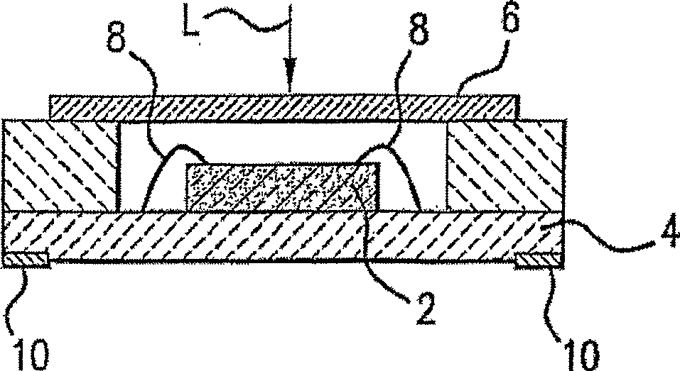
[0031] A photosensitive semiconductor wafer has a plurality of chips and, as in other semiconductor wafers, each chip has an integrated circuit formed on the front side of the wafer. Each chip has multiple bonding pads. The front side of the wafer has a patterned passivation layer to protect the underlying integrated circuits. There is an opening in the passivation layer on the welding pad. Each such photosensitive chip has at least one photosensitive area on the front side.

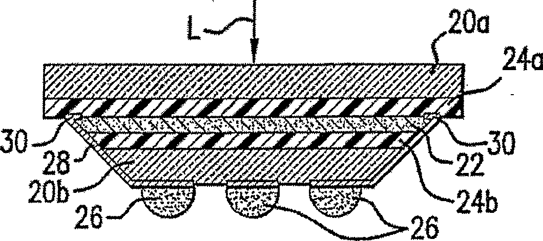
[0032]Wafer bumping technology is well known (as described in US Patent No. 3,292,240, later assigned to IBM, entitled "Method of Fabricating Microfunctional Components"), and has been widely used since its inception. A typical wafer bumping process includes at least one patterned metal layer to form solder bump pads that are attached to the pads of the wafer. Alloys used for solder bump pads are usually referred to as under-bump alloys (UBM) and are often multilayered to provide multiple functions su...


PUM


Abstract

A photo-sensing device package and the method of packaging such device is provided. The package includes an assembly portion having a substrate formed of a material substantially transparent to light within a predetermined range of wavelengths; a sensing portion including at least one photo-sensing die photo-electronically transducing light within the predetermined range of wavelengths; and, a plurality of first solder joints joining the sensing and assembly portions. The assembly portion is formed with at least a first metal layer disposed on the substrate about a front surface region thereof; and, at least one passivation layer formed to extend over the first metal layer. The package is cheap and compact, and simply fabricated.

Description

technical field [0001] The present invention generally relates to an electronic package of a semiconductor integrated circuit, and more particularly, relates to an electronic package of a photosensitive semiconductor device. Background technique [0002] Light-sensitive semiconductor devices are usually mounted in ceramic packages. figure 1 A schematic cross-sectional view of a ceramic leadless chip carrier (CLCC), which is the most common form of packaging for light-sensing devices, is shown. As shown in the figure, inside the area covered by the glass cover 6 , the light-sensing semiconductor chip is fixed on the ceramic substrate 4 with the front facing up by using epoxy material or similar material. Soldering wires 8 are generally used to connect the photosensitive chip 2 to the ceramic substrate 4 . Solderable pads 10 are provided on the bottom of the ceramic substrate 4 to connect the package to a circuit board. [0003] Perhaps the most important drawback of this p...

Claims


Application Information

Patent Timeline
Patent Type & Authority Patents(China)
IPC IPC(8): H01L27/14
Inventor 金德勋约翰·J·H·雷歇
Owner OPTOPAC
Why Eureka
Try Eureka