Semiconductor device having flip-chip package and method for fabricating the same

a semiconductor device and flip-chip technology, applied in semiconductor devices, semiconductor/solid-state device details, electrical equipment, etc., can solve the problems of increasing fabrication costs, inconvenient, and high cost of build-up substrates, and achieve the effect of reducing the overall thickness of the fabricated produ

Inactive Publication Date: 2006-05-11
SILICONWARE PRECISION IND CO LTD
View PDF14 Cites 39 Cited by
  • Summary
  • Abstract
  • Description
  • Claims
  • Application Information

AI Technical Summary

Benefits of technology

[0023] In a further preferred embodiment of the present invention, the flip-chip package is mounted on the carrier in a manner that external connection contacts of the build-up substrate face upwardly, and the inactive surface of the firs...

Problems solved by technology

A conventional method uses bonding wires such as gold wires to electrically connect the chip to the chip carrier, which is not suitable as being limited by trace routability.
As a pitch between the adjacent solder bumps generally ranges from 150 to 250 μm and is quite small, a build-up substrate must be used as the chip carrier to provide corresponding bump pads for bonding the solder bumps on the chip, which however increases fabrication costs as the build-up substrate is expensive.
The bridging effect of the solder bumps lead to short circuit, thereby degrading the yield of a fabricated flip-chip semiconductor package.
Although the flip-chip semiconductor package is suitable for incorporating the highly integrated chip, it is still not able to provide satisfactory performance for an advanced electronic product.
As the build-up substrate is expensive, the use of a build-up substrate with a large area i...

Method used


Image

  • Semiconductor device having flip-chip package and method for fabricating the same
  • Semiconductor device having flip-chip package and method for fabricating the same
  • Semiconductor device having flip-chip package and method for fabricating the same

Examples


first preferred embodiment

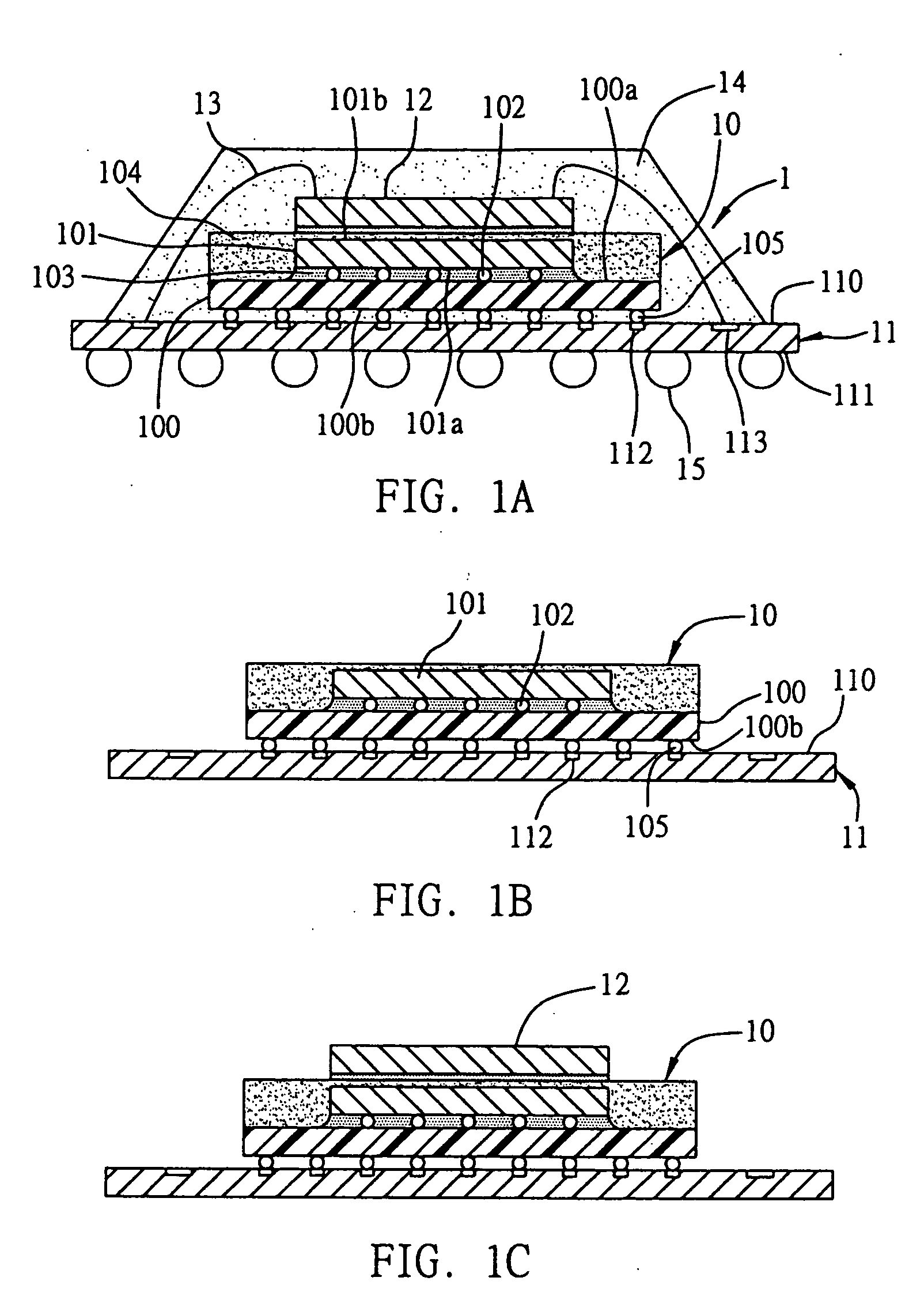
[0036]FIG. 1A is a cross-sectional view showing a semiconductor device having a flip-chip package according to a first preferred embodiment of the present invention. FIGS. 1B to 1E are cross-sectional views showing a method for fabricating the semiconductor device shown in FIG. 1A.

[0037] As shown in FIG. 1A, the semiconductor device 1 of the first preferred embodiment comprises a flip-chip package 10; a carrier 11 for mounting and electrically connecting the flip-chip package 10; a second chip 12 mounted on the flip-chip package 10; a plurality of gold wires 13 for electrically connecting the second chip 12 to the carrier 11; a second encapsulant 14 formed on the carrier 11 for encapsulating the flip-chip package 10, the second chip 12 and the gold wires 13; and a plurality of array-arranged solder balls 15 implanted on the carrier 11.

[0038] The flip-chip package 10 comprises a build-up substrate 100 having a first surface 100a and a corresponding second surface 100b; a first chip...

second preferred embodiment

[0050]FIG. 2 is a cross-sectional view showing a semiconductor device having a flip-chip package according to a second preferred embodiment of the present invention.

[0051] Referring to FIG. 2, the semiconductor device 2 having a flip-chip package in the second preferred embodiment is structurally similar to that in the first preferred embodiment, with the difference in that for the semiconductor device 2, an inactive surface 201b of a first chip 201 encapsulated in a flip-chip package 20 is exposed from a first encapsulant 204 formed on a build-up substrate 200 for mounting the first chip 201. After the flip-chip package 20 is mounted on a carrier 21, a second chip 22 can be directly attached to the inactive surface 201b of the first chip 201. Therefore, an overall thickness of the fabricated semiconductor device 2 is smaller than that of the semiconductor device 1 in the first preferred embodiment.

[0052] Besides, in order to further reduce the thickness of the flip-chip package 2...

third preferred embodiment

[0053]FIG. 3 is a cross-sectional view showing a semiconductor device having a flip-chip package according to a third preferred embodiment of the present invention.

[0054] Referring to FIG. 3, the semiconductor device 3 having a flip-chip package in the third preferred embodiment is structurally similar to that in the second preferred embodiment, with the difference in that for the semiconductor device 3, after a flip-chip package 30 is fabricated, a heat spreader 36 made of a metal material is mounted on the flip-chip package 30, such that an inactive surface 301b of a first chip 301 exposed from a first encapsulant 304 in the flip-chip package 30 can be directly attached to the heat spreader 36. After the flip-chip package 30 mounted with the heat spreader 36 is electrically connected to a carrier 31 by a plurality of solder balls 305, a second chip 32 is directly attached to the heat spreader 36. Therefore, the first chip 301 and the second chip 32 of the semiconductor device 3 a...


PUM


Abstract

A semiconductor device having a flip-chip package and a method for fabricating the same are provided. A flip-chip package after being tested to be functionally workable is mounted on a carrier and is electrically connected to the carrier by a plurality of first conductive elements, the flip-chip package having a first chip mounted on a substrate in a flip-chip manner. At least a second chip is mounted on the flip-chip package and is electrically connected to the carrier by a plurality of second conductive elements. An encapsulant is formed on the carrier for encapsulating the flip-chip package and the second chip. A plurality of solder balls are implanted on a bottom surface of the carrier, such that the first and second chips can be electrically connected to an external device via the solder balls. The above arrangement can effectively improve the yield of a fabricated product and reduce packaging costs.

Description

FIELD OF THE INVENTION [0001] The present invention relates to ball grid array (BGA) semiconductor devices and methods for fabricating the same, and more particularly, to a multi-chip BGA semiconductor device and a method for fabricating the semiconductor device. BACKGROUND OF THE INVENTION [0002] Besides profile miniaturization, a present electronic product is required to have multiple functions and a high operation speed, and such requirements are usually satisfied by incorporating a highly integrated chip in the electronic product. The high integration of the chip increases the number of input / output (I / O) connections on the chip used for electrically connecting the chip to a chip carrier. A conventional method uses bonding wires such as gold wires to electrically connect the chip to the chip carrier, which is not suitable as being limited by trace routability. Accordingly, a flip-chip method using a plurality of array-arranged solder bumps formed on an active surface of the chip...

Claims


Application Information

Patent Timeline
IPC IPC(8): H01L23/52H01L23/48
CPCH01L23/3128H01L23/3135H01L25/03H01L2224/48137H01L2924/01079H01L2924/15311H01L24/48H01L2224/45144H01L2924/00H01L2224/73265H01L2224/32225H01L2224/48227H01L2224/73204H01L2224/16225H01L2224/32145H01L2224/32245H01L2224/48145H01L2224/73253H01L2924/19107H01L2924/00012H01L2924/00014H01L24/45H01L24/73H01L2924/181H01L2924/00011H01L2924/00015H01L2224/05599H01L2224/0401
Inventor PU, HAN-PINGHUANG, CHIEN-PING
Owner SILICONWARE PRECISION IND CO LTD
Why Eureka
Try Eureka