Electronic package of photo-sensing semiconductor devices, and the fabrication and assembly thereof

a technology of photo-sensing semiconductor devices and electronic packages, which is applied in the direction of semiconductor devices, semiconductor/solid-state device details, radiation control devices, etc., can solve the problems of limited improvements in positioning accuracy of photo-sensing devices, package configurations that do not allow very precise placement of photo-sensing devices, and small packaging sizes for hand-held applications. , to achieve the effect of reducing packaging costs

Active Publication Date: 2005-03-08
OPTOPAC
View PDF9 Cites 37 Cited by
  • Summary
  • Abstract
  • Description
  • Claims
  • Application Information

AI Technical Summary

Benefits of technology

A substrate is fabricated separately. This substrate may be configured, for example, as a circular wafer or a rectangular panel. This substrate will have a plurality of unit substrates in much the same manner as the semiconductor wafer having a plurality of dice. Each unit substrate becomes an assembly portion which, together with the sensing portion, forms the electronic package after fabrication and assembly are complete. The material for the substrate is preferably transparent at the wavelength of light where the photo-sensing devices respond. Borosilicate glass is one example of a material having sufficient transparency for photo-sensing devices in the visible portion of the spectrum. The fabrication of this substrate includes forming at least one patterned metal layer to make solder bump pads and interconnection lines between the solder bump pads by deposition and patterning using any suitable measures known to persons versed in semiconductor fabrication art. These solder bump pads are grouped into at least two sets. The solder bump pads in the first set are relatively smaller and correspond to the solder bumps of the photo-sensing dice for making interconnections to those photo sensing dice. The solder bump pads in the second set are relatively larger and are used for making interconnections of the resulting package itself to external circuits, such as supporting printed circuit board. Also, the substrate includes at least one patterned passivation layer over the patterned metal layer for protecting the interconnection lines formed thereby. This patterned passivation layer has openings at the solder bump pads. Preferably, the substrate also includes a patterned dust-seal layer over the patterned passivation layer around the photo-sensing area for preventing dust particles from entering the area.
While a CLCC package requires a ceramic substrate for interconnection and a glass lid for light transmission, a package formed in accordance with the present invention requires only a glass substrate having both functions. Also, the present invention employs batch processes such as wafer bumping for photo-sensing device wafer. It similarly employs batch processes for the fabrication and assembly of the substrate having a plurality of unit substrates. As a result of this simplification and batch processing, the present invention decreases packaging costs significantly. Unlike certain packaging techniques heretofore known, for instance, the present invention uses flipchip mounting which is a simple and field proven technique instead of very complicated processes that require extending bonding pads onto dicing areas, thinning of the wafer, and removing of silicon to expose the metal on dicing areas. Also, such features as flipchip mounting of photo-sensing dice onto a substrate and the use and arrangement of solder bumps for the disclosed package provide consistent and precise, guided positioning of a focal plane in the horizontal and vertical directions in an effortless manner. Self-alignment effectively occurs during the solder reflow process.

Problems solved by technology

Perhaps the most critical drawback of this package is that it is very expensive.
Another drawback is that the package size is not small enough for some hand-held applications such as cameras in cellular phones where small size and light weight are essential features.
Another drawback is that the package's configuration does not allow very precise placement of the photo-sensing device in relation, for instance, to the focal plane of a lens because, among other things, the photo-sensing die is mounted with epoxy or the like, and the package itself is mounted with solder paste.
The aforementioned Patent provides limited improvements in positioning accuracy for the sensor with respect to its primitive lens system.
It also provides at best mediocre accuracy in the placement of the package itself on a mounting board.
Perhaps the most critical drawback with this package is the complexity both in structure and fabrication process.
This complexity is a significant factor in mass production since complexity tends to increase the processing yield loss.
As a result of its complexity and attendant yield loss, the package is expensive to fabricate.
Other nontrivial disadvantages of this technique include its need for a wide dicing line, which cuts against the trend in semiconductor manufacturing to decrease the width of dicing lines to achieve more dice per wafer.
The current typical dicing line width of about 100 micrometers is not wide enough to support this technique.
Consequently, the packaging technique is not compatible with semiconductor wafers having standard dicing line widths, and requires customizing measures to ensure the wider than usual dicing line widths.

Method used


Image

  • Electronic package of photo-sensing semiconductor devices, and the fabrication and assembly thereof
  • Electronic package of photo-sensing semiconductor devices, and the fabrication and assembly thereof
  • Electronic package of photo-sensing semiconductor devices, and the fabrication and assembly thereof

Examples


Embodiment Construction

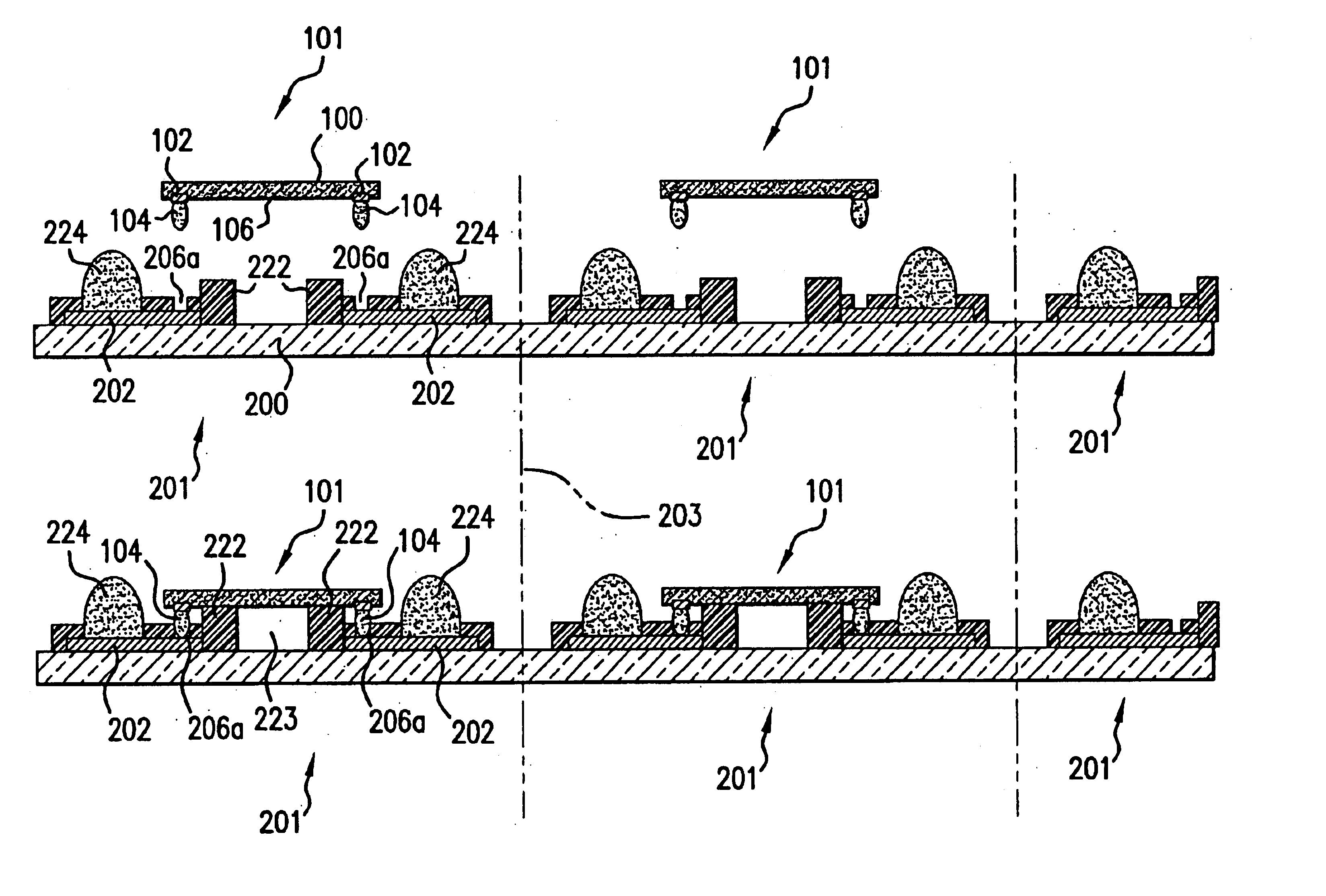
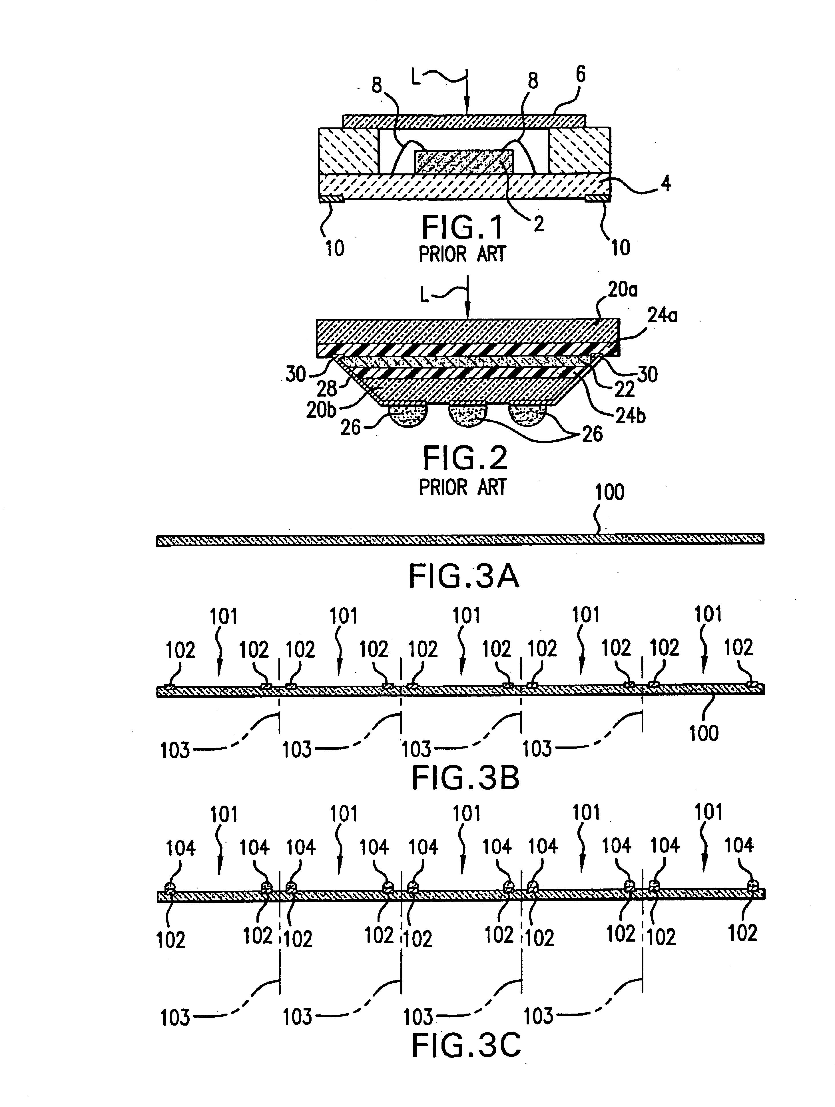
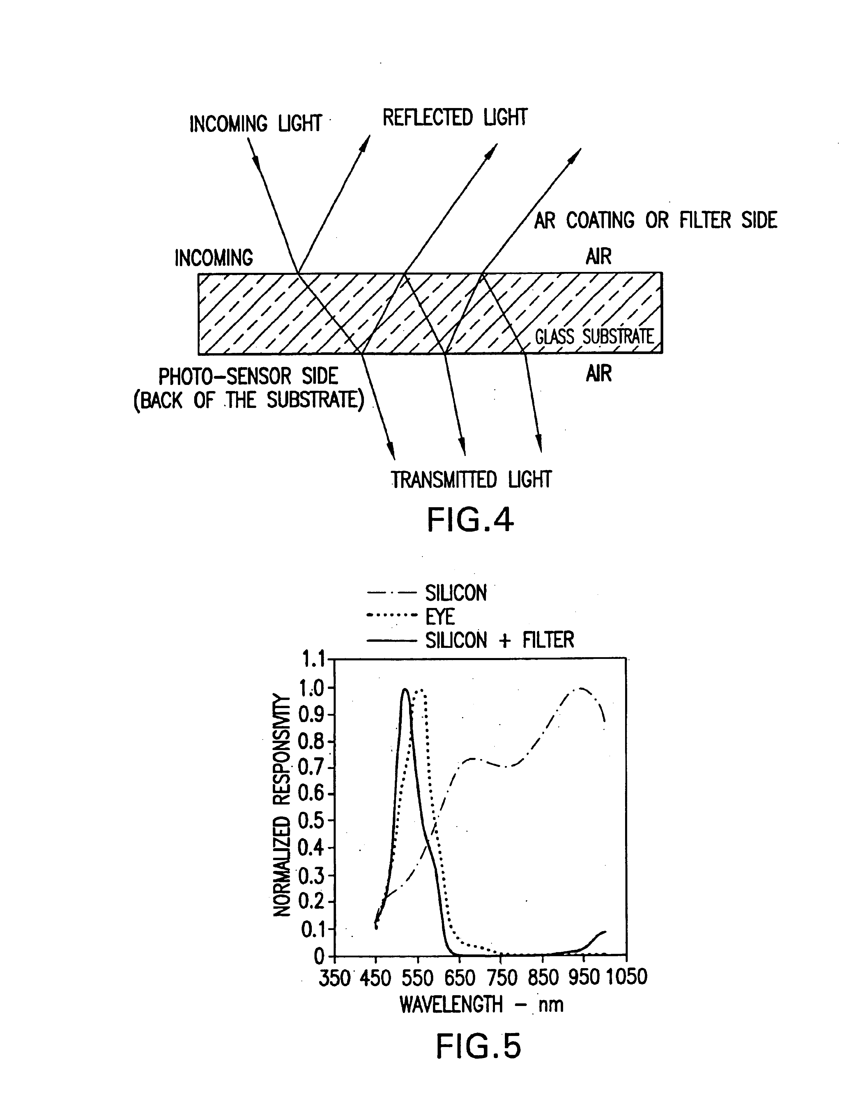
A photo-sensing semiconductor wafer has a plurality of dice, and each die has integrated circuitry formed on a front surface of the wafer, much as in other semiconductor wafers. Each die has a plurality of bonding pads. The wafer has a patterned passivation layer over the front surface for protecting the integrated circuitry underneath. The passivation layer has openings on said bonding pads. Each such photo-sensing die has at least one photo-sensing area on a front surface.

Wafer bumping is a well-known technique that has been widely used since its initial teaching, as reflected in U.S. Pat. No. 3,292,240 entitled “Method of Fabricating Microminiature Functional Components,” assigned to IBM. A typical wafer bumping process includes at least one patterned metal layer for making solder bump pads connected to bonding pads on the wafer. Metallurgy used for solder bump pads is commonly referred to as under bump metallurgy (UBM) and typically utilizes a multilayered structure to provide m...


PUM


Abstract

A photo-sensing device package and the method of packaging such device is provided. The package includes an assembly portion having a substrate formed of a material substantially transparent to light within a predetermined range of wavelengths; a sensing portion including at least one photo-sensing die photo-electronically transducing light within the predetermined range of wavelengths; and, a plurality of first solder joints joining the sensing and assembly portions. The assembly portion is formed with at least a first metal layer disposed on the substrate about a front surface region thereof; and, at least one passivation layer formed to extend over the first metal layer. The passivation layer is patterned to define a plurality of first and second access openings which respectively describe on the first metal layer a plurality of first and second solder bump pads, each of which is interconnected to at least one of the second solder bump pads. The sensing portion's photo-sensing die is positioned with its photo-sensing area opposing the front surface region of the assembly portion's substrate, and has formed thereon a plurality of solder bump pads electrically coupled to the photo-sensing area. Each of the first solder joints extends between one of the sensing portion's solder bump pads and one of the assembly portion's first solder bump pads.

Description

PRIOR ARTPhoto-sensing semiconductor devices have been typically mounted in ceramic packages. FIG. 1 shows a schematic cross-section view of a ceramic leadless chip carrier (CLCC), which is the most popular package format for photosensing devices. As shown in the figure, a photo sensing semiconductor die is mounted face-up on a ceramic substrate 4 by using epoxy or the like inside of an enclosure that is covered by a glass lid 6. Wire bonding 8 is typically used to connect the photo-sensing die 2 to the ceramic substrate 4. Solderable pads 10 are provided on the bottom of ceramic substrate 4 to connect the package to a circuit board.Perhaps the most critical drawback of this package is that it is very expensive. Another drawback is that the package size is not small enough for some hand-held applications such as cameras in cellular phones where small size and light weight are essential features. Another drawback is that the package's configuration does not allow very precise placeme...

Claims


Application Information

Patent Timeline
Patent Type & Authority Patents(United States)
IPC IPC(8): H01L21/00H01L21/02H01L21/30H01L27/14H01L21/46H01L29/40H01L23/48H01L23/00H01L27/148H01L31/0203
CPCH01L27/14618H01L31/0203H01L2224/48091H01L2924/00014H01L2924/16195H01L27/148H01L23/00
Inventor KIM, DEOK HOONRECHE, JOHN J. H.
Owner OPTOPAC
Why Eureka
Try Eureka