Boron nitride pyrolyzing crucible coating method

A crucible and surface technology, applied in the field of PBN crucible surface treatment, can solve the problems of increasing industrial production cost, layering, and not being able to solve the service life of PBN crucible well

Active Publication Date: 2009-06-03
云南中科鑫圆晶体材料有限公司
View PDF5 Cites 0 Cited by
  • Summary
  • Abstract
  • Description
  • Claims
  • Application Information

AI Technical Summary

Problems solved by technology

After each crystal growth, the inner wall of the PBN crucible has a large area of ​​peeling and even stratification. This method cannot solve the problem of the service life of the PBN crucible well. At the same time, the contamination of the PBN crucible by impurities in the air will also directly affect the body. single crystal quality
Moreover, the high breakage rate of the PBN crucible also increases the cost of industrial production

Method used


Image

  • Boron nitride pyrolyzing crucible coating method

Examples


Embodiment Construction

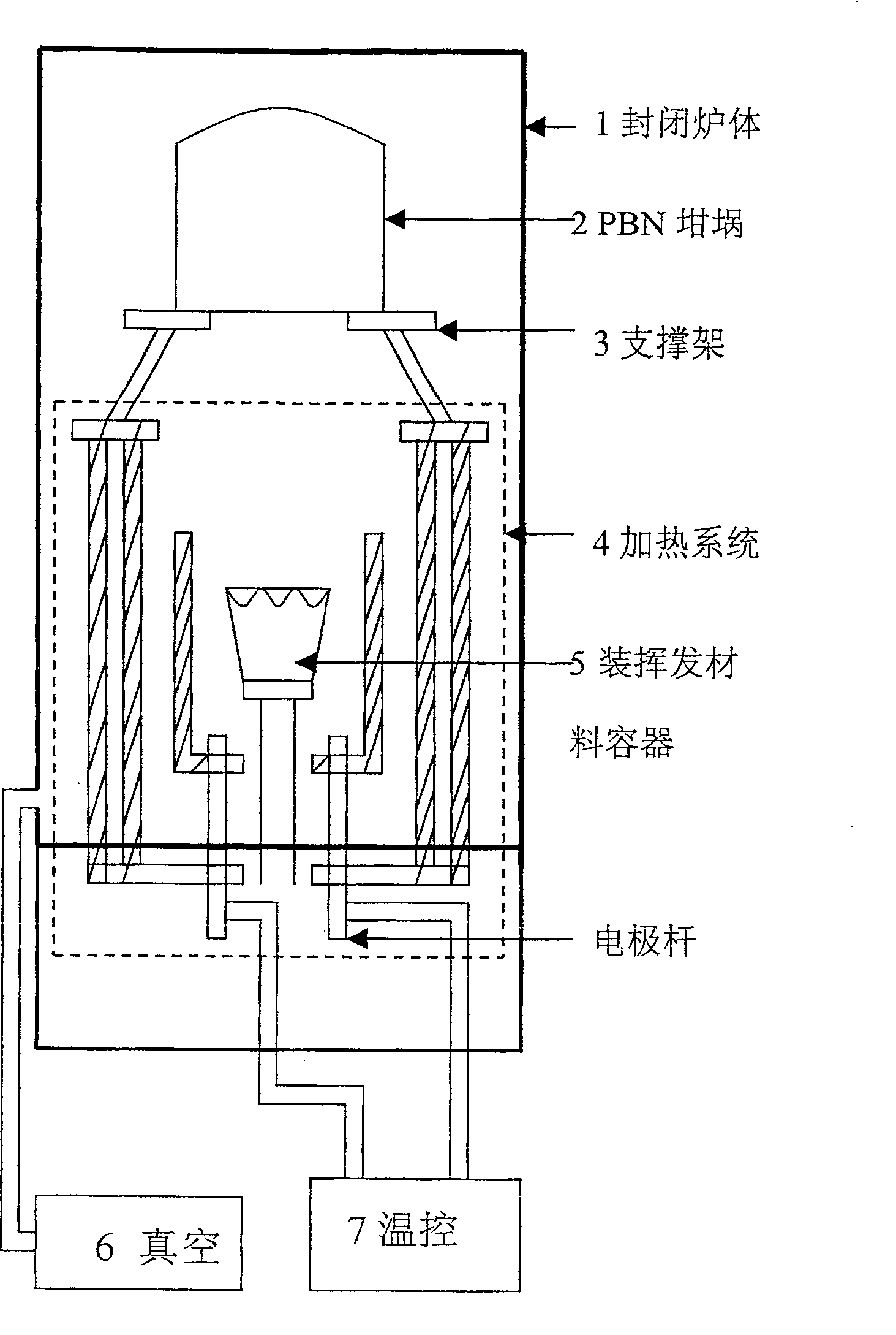
[0020] see figure 1 Shown, the PBN crucible surface coating of the present invention comprises:

[0021] 1. Equipment

[0022] The container (5) for containing the volatile material is located in the center of the closed furnace chamber (1), and is made of high temperature resistant material, which does not react with the volatile material. Volatile materials can form a thin film on the surface of the PBN(2) crucible without affecting the quality of the bulk single crystal. The PBN (2) crucible is on the support system (3) at the top of the closed furnace chamber (1).

[0023] A set of heating system (4) and temperature control equipment (7) are used to heat up the temperature, so that the volatile material is diffused to the surface layer of the PBN crucible for deposition. The heating system (4) is around the closed furnace chamber (1).

[0024] A support system (3) supports the PBN crucible (2) and requires high temperature resistance.

[0025] A closed furnace chamber...


PUM


Abstract

The present invention belongs to the field of semiconductor technology, and is especially coating method and apparatus for the surface of PBN crucible for LEC process monocrystal growth. The coating apparatus includes one container for holding volatile material, one heating system with temperature control device, one support system, and one closed furnace with corresponding vacuum equipment to provide volatilizing space. The coating method is that under the basis of traditional technological process and by means of heating and temperature control with the heating system with temperature control device, B2O3 with high water content is dewatered, volatilized and diffused to the surface of PBN crucible at the low temperature end to form B2O3 film.

Description

technical field [0001] The invention belongs to the technical field of semiconductors, in particular to a method and a device for treating the surface layer of a PBN crucible in the preparation process for growing bulk single crystals by the LEC method. Background technique [0002] Semiconductor materials are the foundation of the information society and are widely used in the fields of electronic information and optical communications. III-V compound semiconductor materials occupy an important position in the cutting-edge scientific field due to their specific properties, among which gallium arsenide and indium phosphide are used as the basis for the development of ultra-high-speed integrated circuits, microwave monolithic circuits, optoelectronic devices and their optoelectronic integration Materials have received a lot of attention. [0003] In the early 1980s, the LEC technology was developed internationally, that is, in the high-pressure single crystal furnace, the ra...

Claims


Application Information

Patent Timeline
Patent Type & Authority Patents(China)
IPC IPC(8): C23C14/08C23C14/24C30B15/00F27B14/10
Inventor 高永亮惠峰王文军
Owner 云南中科鑫圆晶体材料有限公司
Why Eureka
Try Eureka