TFT LCD array substrate structure and its producing method

An array substrate structure and manufacturing method technology, applied in semiconductor/solid-state device manufacturing, optics, instruments, etc., can solve problems such as the reduction of aperture ratio, and achieve the effects of reducing jump voltage, increasing aperture ratio, and increasing signal stability

Active Publication Date: 2009-06-10
BOE TECH GRP CO LTD +1
View PDF6 Cites 0 Cited by
  • Summary
  • Abstract
  • Description
  • Claims
  • Application Information

AI Technical Summary

Problems solved by technology

Since the drain electrode is always in the pixel area, a part of the aperture ratio will always be sacrificed, resulting in a decrease in the aperture ratio. Usually, the way to increase the aperture ratio is to compress the area of ​​other parts to increase the aperture ratio.

Method used


Image

  • TFT LCD array substrate structure and its producing method
  • TFT LCD array substrate structure and its producing method
  • TFT LCD array substrate structure and its producing method

Examples


Embodiment Construction

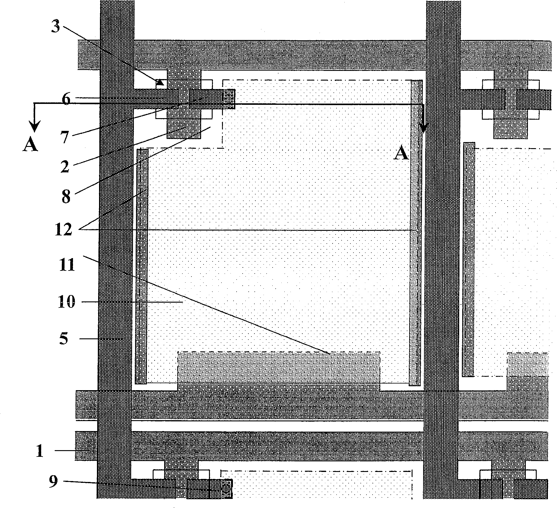
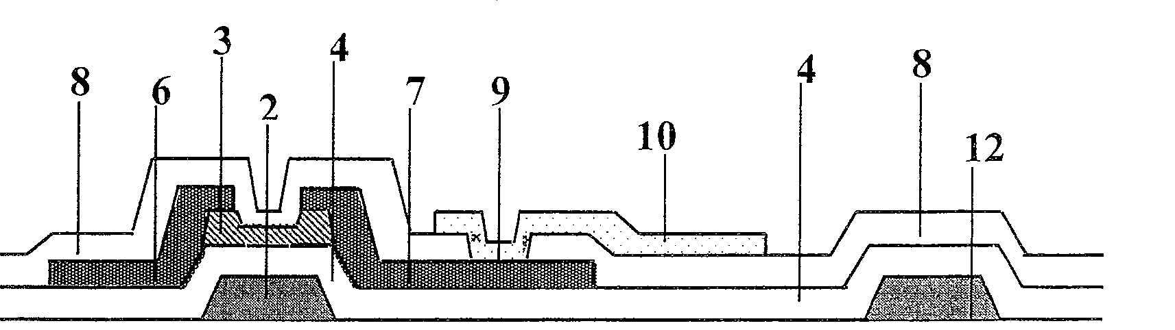
[0042] image 3 Shown is a top view of a specific embodiment of the TFT LCD array substrate structure of the present invention. like image 3 As shown, the array substrate of the TFT LCD has a group of gate scanning lines 1 and common electrodes 13 parallel thereto, and a group of data scanning lines 5 perpendicular thereto. Adjacent gate scan lines 1 and data scan lines 5 define pixel regions. Each pixel includes a TFT switch device, a transparent pixel electrode 10 and a part of the common electrode 13 . like Figure 3a As shown, the TFT device is composed of a gate electrode 2 , a gate electrode insulating layer 4 , an active layer 3 , and a source electrode 6 and a drain electrode 7 . The transparent pixel electrode 10 is connected to the drain electrode 7 of the TFT through the passivation layer via hole 9 . The above part is the same as a traditional TFT pixel structure. The TFT LCD pixel structure of the present invention is different in that the present invention...


PUM


Abstract

This invention provides a TFT LCD array base plate structure including a base plate, a light strip, a grid insulation layer, a data scanning line, a film transistor, a passivation layer and its trough hole or groove formed on the drain of the film transistor, a pixel electrode formed on the passivation layer connected with the drain via the through hole or the groove, in which, the light strip is placed around the pixel electrode. This invention also provides a manufacturing method for the TFT LCD array base plate structure, which forms a close light strip around the pixel electrode the same time when forming grid scanning lines.

Description

technical field [0001] The invention relates to a thin film transistor liquid crystal display (TFT LCD), in particular to a thin film transistor liquid crystal display array substrate structure and a manufacturing method thereof. Background technique [0002] Among flat panel display technologies, TFT LCD has the characteristics of low power consumption, relatively low manufacturing cost, and no radiation, and thus occupies a dominant position in the flat panel display market. TFT LCD devices are formed by combining array glass substrates and color filter glass substrates. like figure 1 Shown is a cross-sectional schematic diagram of a current mainstream amorphous silicon TFT (thin film transistor) structure and a top view of a single pixel. It is a bottom gate structure with back channel etching. As shown in the figure, the array structure includes: a group of gate scanning lines 1 and a group of data scanning lines 5 perpendicular thereto, and adjacent gate scanning lin...

Claims


Application Information

Patent Timeline
Patent Type & Authority Patents(China)
IPC IPC(8): H01L27/12H01L23/522H01L21/84H01L21/768G02F1/136
CPCH01L27/1214G02F1/136227H01L27/124H01L27/1248
Inventor 明星张弥
Owner BOE TECH GRP CO LTD
Why Eureka
Try Eureka