Amplification type solid state imaging device

A solid-state imaging device, a large-scale technology, applied in the direction of electric solid-state devices, semiconductor devices, electrical components, etc., can solve the problems of image quality degradation, noise removal performance, etc., and achieve the effect of suppressing the degradation of image quality

Active Publication Date: 2009-06-17
PANASONIC SEMICON SOLUTIONS CO LTD
View PDF5 Cites 0 Cited by
  • Summary
  • Abstract
  • Description
  • Claims
  • Application Information

AI Technical Summary

Problems solved by technology

In addition, since the generated current locally affects the noise removal performance, there is a problem of deteriorating image quality as a result.

Method used


Image

  • Amplification type solid state imaging device
  • Amplification type solid state imaging device
  • Amplification type solid state imaging device

Examples


no. 1 approach

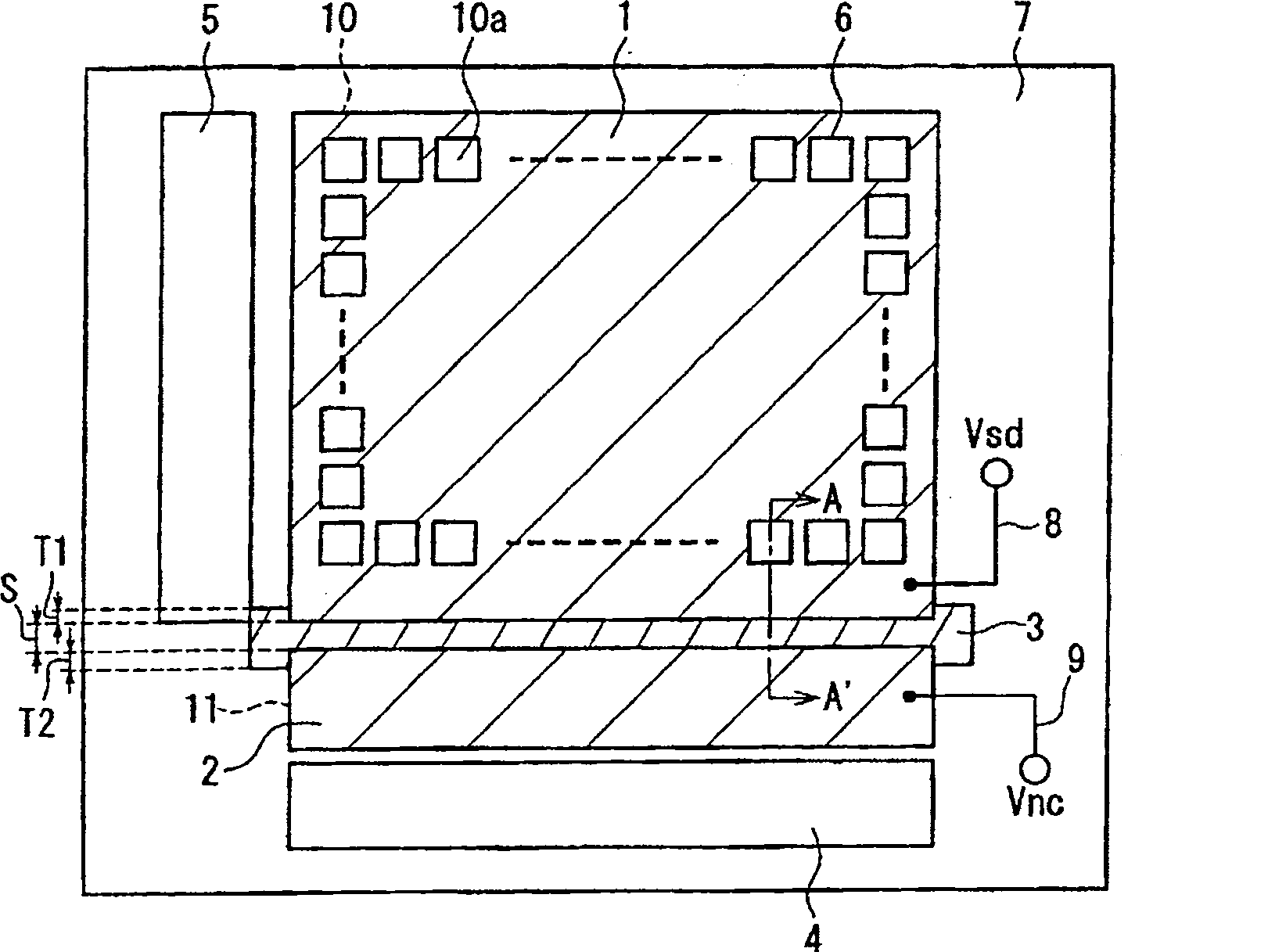
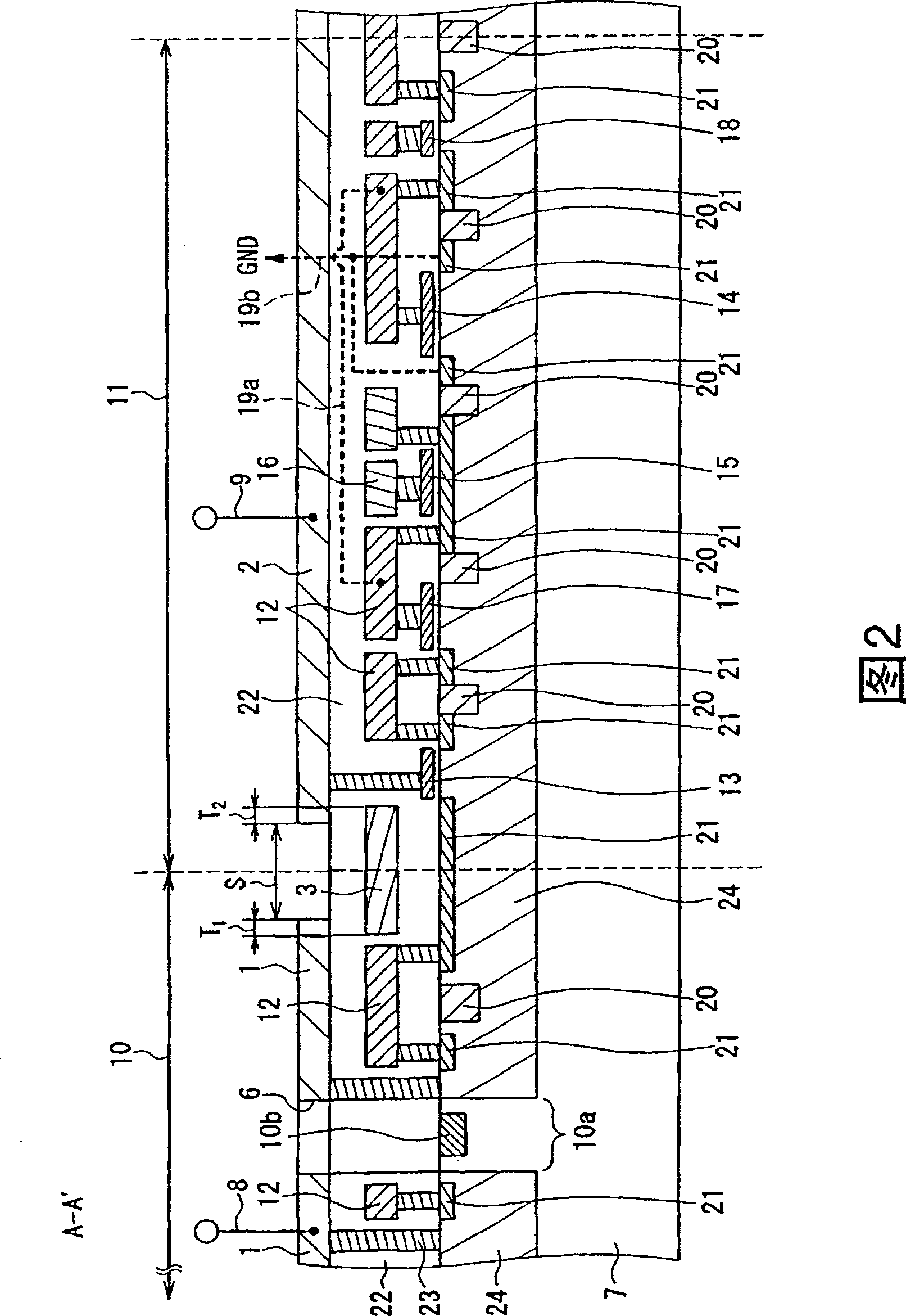
[0046] Below, refer to figure 1 2, the amplifying solid-state imaging device according to the first embodiment of the present invention will be described. figure 1 It is a schematic diagram showing the layout of the amplifying solid-state imaging device according to the first embodiment of the present invention. Figure 2 is a representation of figure 1 A cross-sectional view of a part of the enlarged solid-state imaging device shown, and shows along the figure 1 The state where the section line A-A' in the section is cut. Note that, in FIG. 2 , hatching is omitted for the main portion of the semiconductor substrate 7 and the insulating layer 22 .

[0047] Such as figure 1 As shown, the amplifying solid-state imaging device includes: a light receiving unit 10 , a reading unit, and a noise removal circuit 11 , all of which are provided on a semiconductor substrate 7 . The light receiving unit 10 is formed by arranging a plurality of pixels one-dimensionally or two-dime...

no. 2 approach

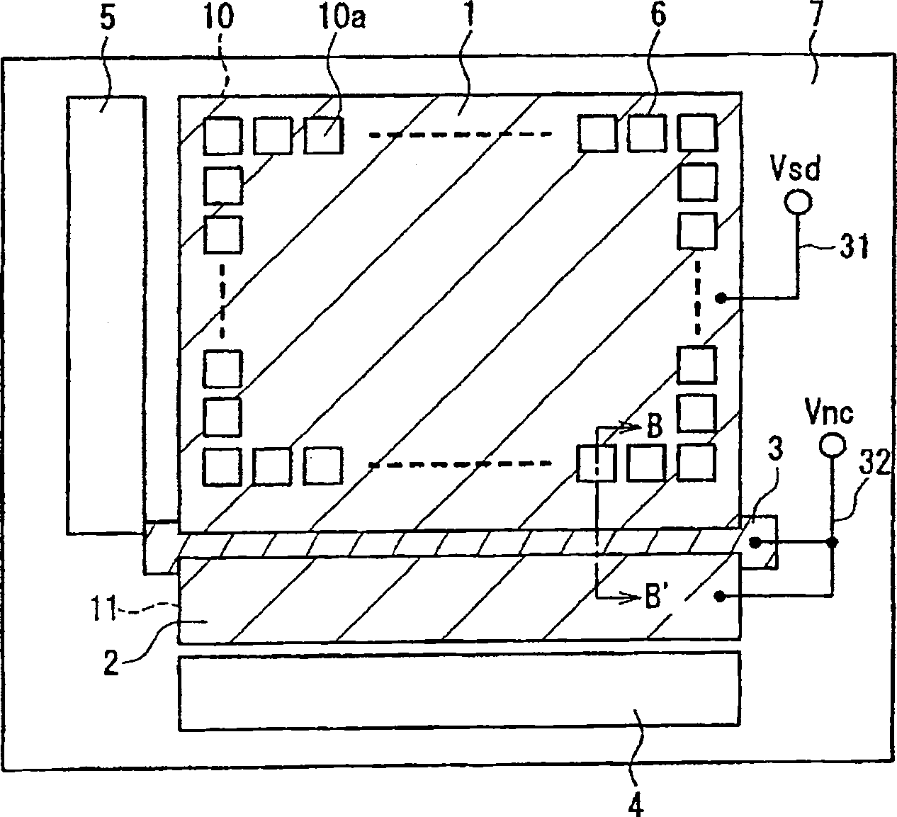
[0072] Next, refer to image 3 4, an amplifying solid-state imaging device in a second embodiment of the present invention will be described. image 3 It is a schematic diagram showing the layout of the amplifying solid-state imaging device according to the second embodiment of the present invention. Figure 4 is a representation of image 3 A cross-sectional view of a part of the enlarged solid-state imaging device shown, and shows along the image 3 The cutting line B-B' in the state.

[0073] again, in image 3 and Figure 4, given the figure 1 or the marked part shown in Figure 2 is with the figure 1 Or the same part as the part given the same mark in FIG. 2 . In addition, in FIG. 4 , hatching is omitted for the main part of the semiconductor substrate 7 and the insulating layer 22 . Also, the parts given the same hatching in FIG. 4 are parts having the same function.

[0074] Such as image 3 As shown in FIG. 4 , the second embodiment is also the same as the firs...

no. 3 approach

[0081] Next, refer to Figure 5 , the amplifying solid-state imaging device in the third embodiment of the present invention will be described. Figure 5 It is a schematic diagram showing the layout of the amplifying solid-state imaging device according to the third embodiment of the present invention. again, in Figure 5 in, endowed with figure 1 The marked parts shown are the same as in the figure 1 The same part as the part assigned the same mark.

[0082] Such as Figure 5 As shown, in this third embodiment, with image 3 Unlike the illustrated example, the second light-shielding layer 2 and the third light-shielding layer 3 are electrically connected by wiring 33 other than the second wiring 32 . Again, for structures other than this, Figure 5 The amplified solid-state imaging device shown has the same image 3 The amplified solid-state imaging device shown has the same structure.

[0083] Specifically, at one side (right side in the figure) end of the second ...


PUM


Abstract

An amplification type solid state imaging device comprising a light receiving section (10) formed by arranging a plurality of pixels for converting incident light into signal charges and outputting an electric signal dependent on the quantity of signal charges one-dimensionally or two-dimensionally on a semiconductor substrate (7), a reading means for reading out electric signals from the plurality of pixels sequentially, a noise removing circuit (11) for suppressing false signal of the electric signals read out by the reading means, and a first light shielding layer (1) located on an upper part of the light receiving section (10) and limiting incidence of light to the part of the pixel other than a photoelectric converting part (10a). A second light shielding layer (2) for limiting incidence of light to the noise removing circuit (11) is further provided on an upper part of the noise removing circuit (11).

Description

technical field [0001] The present invention relates to an amplifying solid-state imaging device. Background technique [0002] refer to Figure 10 A layout design of a conventional amplified solid-state imaging device will be described. like Figure 10 As shown, the amplifying solid-state imaging device is configured by forming a light receiving unit 112, a horizontal scanning unit 114, a vertical scanning unit 115, and a noise removing circuit 120 on a semiconductor substrate 117 (for example, refer to Patent Document 1). [0003] The light receiving unit 112 is configured by arranging a plurality of pixels one-dimensionally or two-dimensionally. In addition, each pixel has a photoelectric conversion unit 112a that converts incident light into signal charges, and an output unit (not shown) that outputs an electrical signal corresponding to the amount of signal charges. exist Figure 10 In the example of , pixels are arranged two-dimensionally. [0004] A light shielding...

Claims


Application Information

Patent Timeline
Patent Type & Authority Patents(China)
IPC IPC(8): H01L27/14H04N5/335H01L27/146H04N5/357H04N5/369H04N5/374H04N5/3745
CPCH04N5/335H01L27/14643H01L27/14609H01L27/14623H04N25/00
Inventor 藤冈崇志桝山雅之稻垣诚
Owner PANASONIC SEMICON SOLUTIONS CO LTD
Why Eureka
Try Eureka