
Multiple layered sheet structured ceramic capacitor

A ceramic capacitor and multi-layer chip technology, which is applied in the direction of laminated capacitors, fixed capacitor electrodes, fixed capacitor dielectrics, etc., can solve the problems that cannot meet the requirements of the electronic technology field, and the anti-electric breakdown strength is not ideal, so as to reduce the breakdown probability, the effect of improving the electric breakdown strength

Inactive Publication Date: 2009-06-24
TSINGHUA TONGFANG CO LTD
View PDF3 Cites 0 Cited by
  • Summary
  • Abstract
  • Description
  • Claims
  • Application Information

AI Technical Summary

Problems solved by technology

Due to the distortion of the fringe electric field between the electrodes in each layer, the disadvantage of this type of ceramic capacitor in application is that its resistance to electrical breakdown is not ideal enough to meet the rapid development of electronic technology.

Method used


Image

  • Multiple layered sheet structured ceramic capacitor
  • Multiple layered sheet structured ceramic capacitor
  • Multiple layered sheet structured ceramic capacitor

Examples


Embodiment Construction

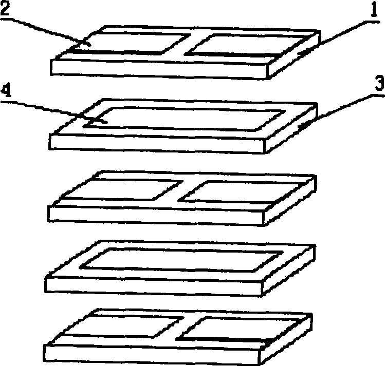
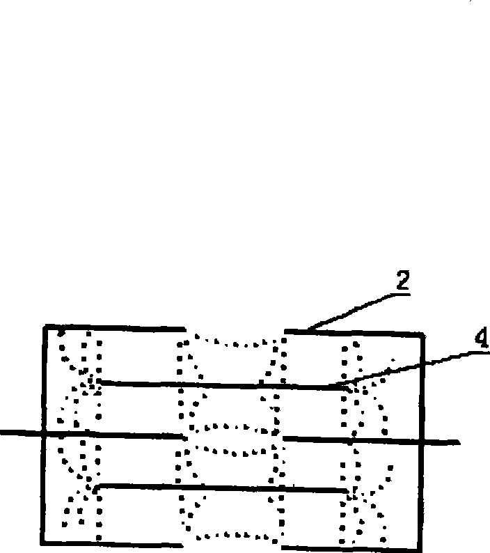
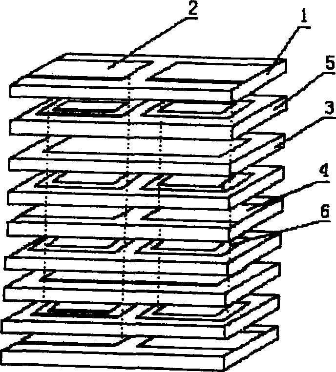
[0014] see image 3 and Figure 4 , The ceramic capacitor of the present invention includes a multi-sheet dielectric in the form of three types of internal electrodes and external electrodes at both ends made of ceramic materials. The internal electrodes 1 and 2 of one type of dielectric layer 1 are two small rectangles arranged at intervals, and the outer edges of each internal electrode 1 and 2 are respectively connected to the external electrodes at both ends; the internal electrodes 2 and 4 of the second type of dielectric layer 3 are in the shape of a The large rectangle corresponds to the printing position of the two small rectangles of the internal electrode 1, and the two ends of the internal electrode on the second type dielectric layer 3 are not connected to the external electrodes; the internal electrode 3 6 of the third type dielectric layer 5 is two frames In a quadrilateral shape, the third internal electrode 6 corresponds to the position of the printed coating ...


PUM


Abstract

A ceramic capacitor with a medium-high voltage multilayer chip structure relates to the technical field of ceramic capacitors. The invention includes several dielectric layers made of ceramic material with two types of internal electrodes and external electrodes at both ends. The internal electrodes of one type of dielectric layer are in two small rectangles arranged at intervals and the outer edges of each internal electrode one are respectively connected to the external electrodes at both ends, and the internal electrodes of the second type of dielectric layer are in a large rectangle connected to the internal electrodes One of the two small rectangles corresponds to the printing position. Its structural feature is that it also includes a dielectric layer in the form of a third type of internal electrode, and the internal electrodes of the third type of dielectric layer are two framed quadrilaterals. The third internal electrode corresponds to the printed coating positions of the first internal electrode and the second internal electrode, and the three types of dielectric layers are placed between the first type of dielectric layer and the second type of dielectric layer, and the above three types of dielectric layers are stacked in sequence. Compared with the prior art, the present invention has the advantage of greatly improving the electric breakdown resistance without changing the dimensions of the ceramic capacitor.

Description

technical field [0001] The invention relates to the technical field of ceramic capacitors, in particular to a ceramic capacitor with a multilayer chip structure suitable for medium and high voltages with a rated voltage above 250V direct current. Background technique [0002] In the technical field of making high-voltage capacitors, two important technical indicators must be considered, one is the size of the capacitor, and the other is the electrical breakdown strength of the capacitor. Although it is now possible to produce capacitors with very small dimensions, it is very difficult to improve their high-voltage breakdown strength without increasing the overall size. The structure of the ceramic capacitor with medium and high voltage multilayer chip structure commonly used in the prior art is made of ceramic materials, consisting of several dielectric layers in the form of two types of internal electrodes and external electrodes at both ends. The internal electrodes of on...

Claims


Application Information

Patent Timeline
Patent Type & Authority Patents(China)
IPC IPC(8): H01G4/30H01G4/005H01G4/12
Inventor 吉岸王晓慧陈仁政张力
Owner TSINGHUA TONGFANG CO LTD
Learn More