
LED chip and thermal sediment direct encapsulated heat radiation component and its making device and method

A technology of LED chips and heat dissipation components, which is applied in the direction of electrical components, semiconductor devices, circuits, etc., can solve the problems such as the structure that is not applicable to the direct packaging of chips and heat dissipation components, so as to facilitate natural convection heat dissipation, improve reliability and life, Effect of reducing thermal resistance

Inactive Publication Date: 2009-07-01
HARBIN INST OF TECH
View PDF4 Cites 0 Cited by
  • Summary
  • Abstract
  • Description
  • Claims
  • Application Information

AI Technical Summary

Problems solved by technology

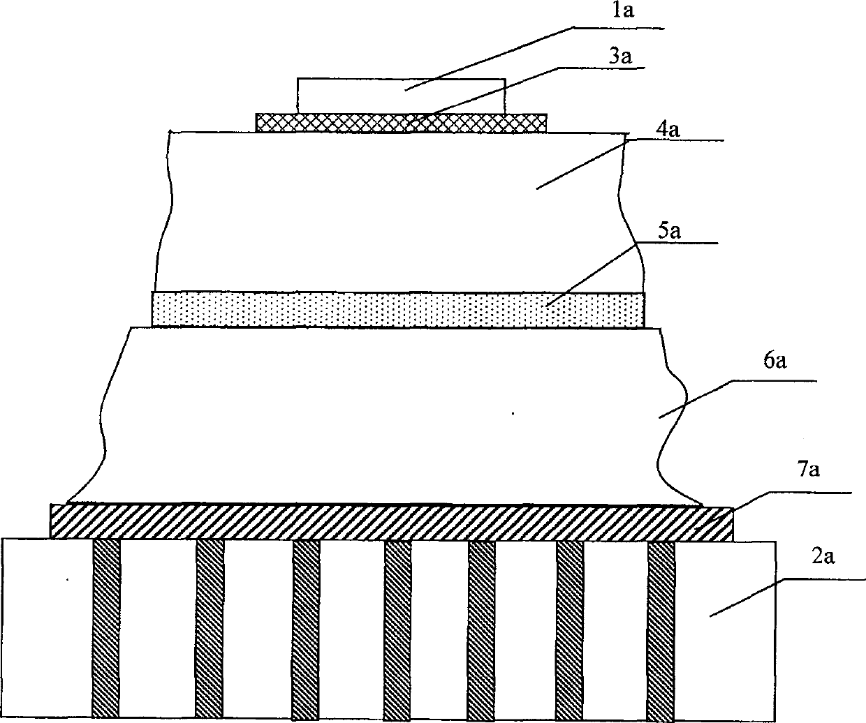
[0005] In order to solve the problem that the packaging method used in the manufacturing process of the existing LED packaging structure is not suitable for the direct packaging structure of the chip and the heat dissipation component, a method for manufacturing the heat dissipation component of the direct packaging of the LED chip and the heat sink is proposed.

Method used


Image

  • LED chip and thermal sediment direct encapsulated heat radiation component and its making device and method
  • LED chip and thermal sediment direct encapsulated heat radiation component and its making device and method
  • LED chip and thermal sediment direct encapsulated heat radiation component and its making device and method

Examples


specific Embodiment approach 1

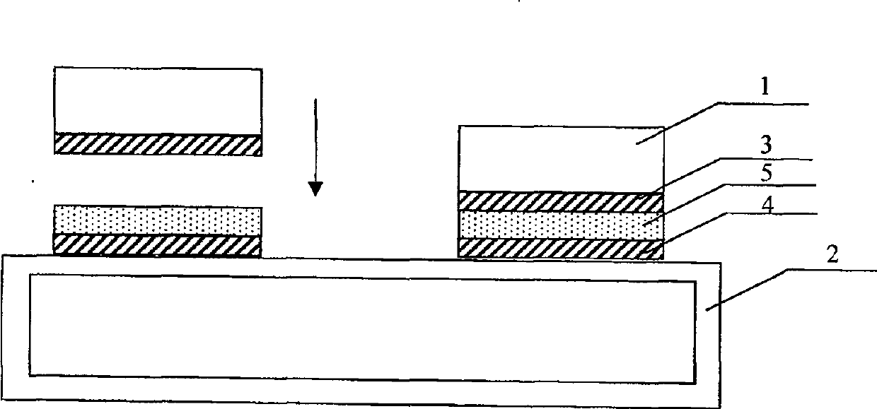
[0016] Specific implementation mode one: combine figure 2 To illustrate this embodiment, the heat dissipation assembly in which the LED chip and the heat sink are directly packaged in this embodiment is composed of an LED chip 1, a rectangular tubular heat sink 2, a chip metal film 3, a heat sink metal film 4 and a solder layer 5; The lower surface of the chip 1 is coated with a chip metal film 3, and the upper surface of the rectangular tubular heat sink 2 is coated with a heat sink metal film 4. The solder layer 5 is placed between the chip metal film 3 and the heat sink metal film 4. The metal film 3 , the heat sink metal film 4 and the solder layer 5 connect the LED chip 1 and the rectangular tubular heat sink 2 .

specific Embodiment approach 2

[0017] Specific implementation mode two: combination figure 2 This embodiment is described. The first difference between this embodiment and the specific embodiment is that the rectangular tubular heat sink 2 is made of copper or aluminum metal. Other compositions and connection methods are the same as those in Embodiment 1.

specific Embodiment approach 3

[0018] Specific implementation mode three: combination figure 2 This embodiment is described. The difference between this embodiment and the first embodiment is that the chip metal film 3 and the heat sink metal film 4 are made of gold Au or silver Ag. Other compositions and connection methods are the same as those in Embodiment 1.


PUM


Abstract

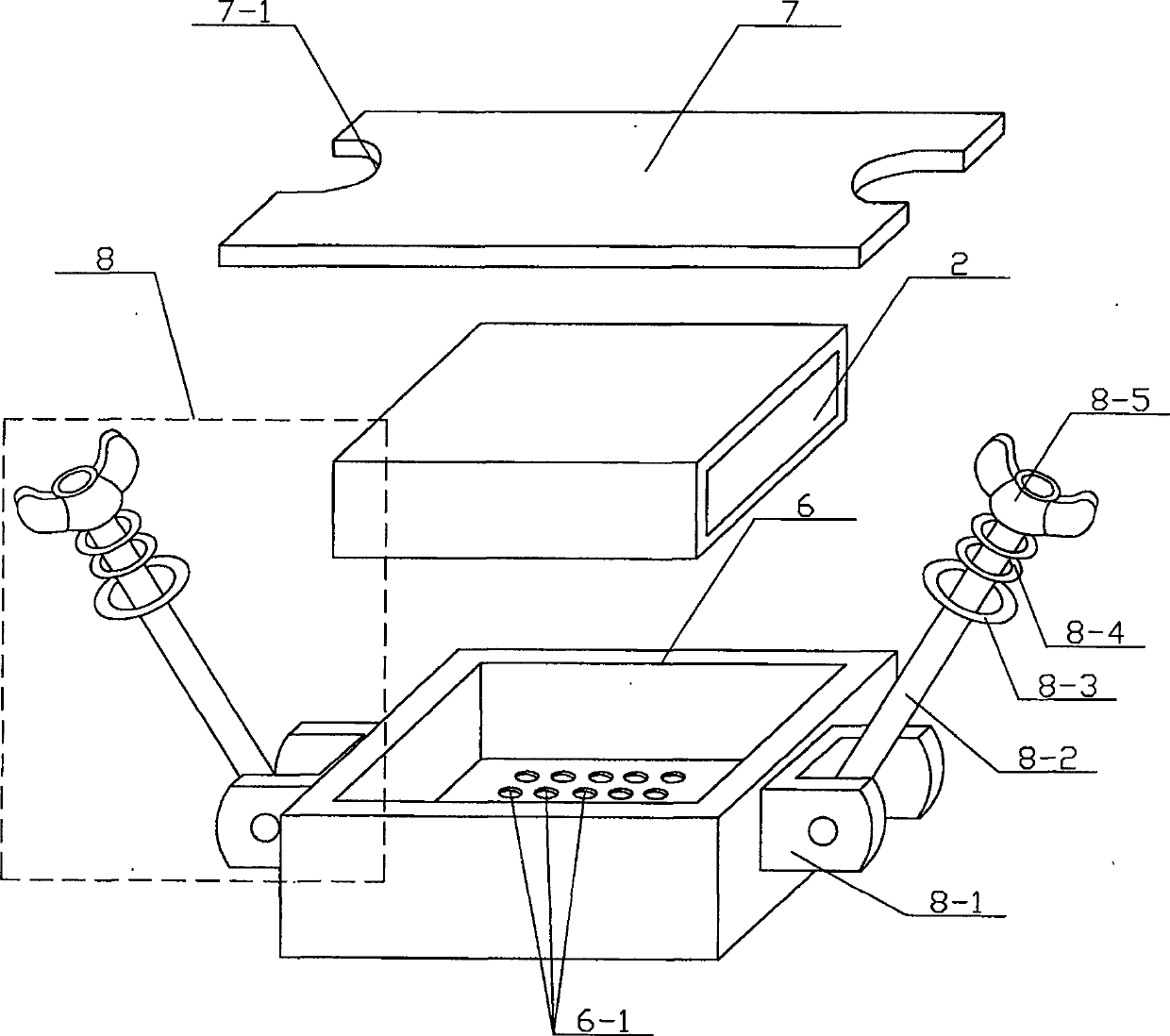
A device for manufacturing a heat dissipation assembly in which LED chips and heat sinks are directly packaged, and the invention relates to the technical field of packaging LED chips and heat sinks. It solves the problem that the encapsulation method adopted in the manufacturing process of the existing LED encapsulation structure is no longer suitable for the direct encapsulation structure of the manufactured chip and the cooling component. The packaging structure and method are as follows: a solder layer is soldered between the LED chip coated with the chip metal film and the rectangular tubular heat sink coated with the heat sink metal film. The manufacturing device is composed of a positioning box, a fixed splint and a fastening component. A set of positioning boxes for placing LED chip chip grooves is arranged on the inner bottom of the box body. A pair of fastening components are respectively installed on the two side walls corresponding to the positioning box. The fixing splint is a rectangular thin plate with horseshoe-shaped notches corresponding to the positions of the fastening components at the edges of the two wide sides. The invention reduces the thermal resistance of the product, so that the heat can be dissipated as soon as possible, improves the saturation current and luminous efficiency of the product, and also improves the reliability and life of the product.

Description

technical field [0001] The invention relates to the technical field of LED chip and heat sink packaging. Background technique [0002] The full name of LED is semiconductor light-emitting diode, which can directly convert electrical energy into light energy. It is characterized by low power consumption, high brightness, bright colors, anti-vibration, long life, cold light source and so on. LED products are widely used, especially with the substantial increase in luminous efficiency and power, various lighting products using LED as light source will inevitably replace incandescent lamps in the 21st century. [0003] Semiconductor components are usually very sensitive to temperature. For high-power LEDs, the driving current is generally above several hundred milliamps, and the temperature rise of the P-N junction is very obvious. Many applications require multiple high-power LEDs to be used in dense arrays. Its heat dissipation problem is particularly prominent. Prolonged h...

Claims


Application Information

Patent Timeline
Patent Type & Authority Patents(China)
IPC IPC(8): H01L33/00
Inventor 王春青孔令超田艳红
Owner HARBIN INST OF TECH
Learn More