Method of manufacturing NAND flash memory device

A memory device and flash technology, applied in the field of NAND flash memory devices, can solve problems such as unit coupling rate and programming speed drop

Inactive Publication Date: 2009-07-15
SK HYNIX INC
View PDF3 Cites 2 Cited by
  • Summary
  • Abstract
  • Description
  • Claims
  • Application Information

AI Technical Summary

Problems solved by technology

[0007] However, if the height of the floating gate decreases, the interference phenomenon between the gates decreases, but the coupling rate and programming speed of the cells decrease

Method used


Image

  • Method of manufacturing NAND flash memory device
  • Method of manufacturing NAND flash memory device
  • Method of manufacturing NAND flash memory device

Examples


Embodiment Construction

[0016] Specific embodiments according to the present invention are described below with reference to the drawings.

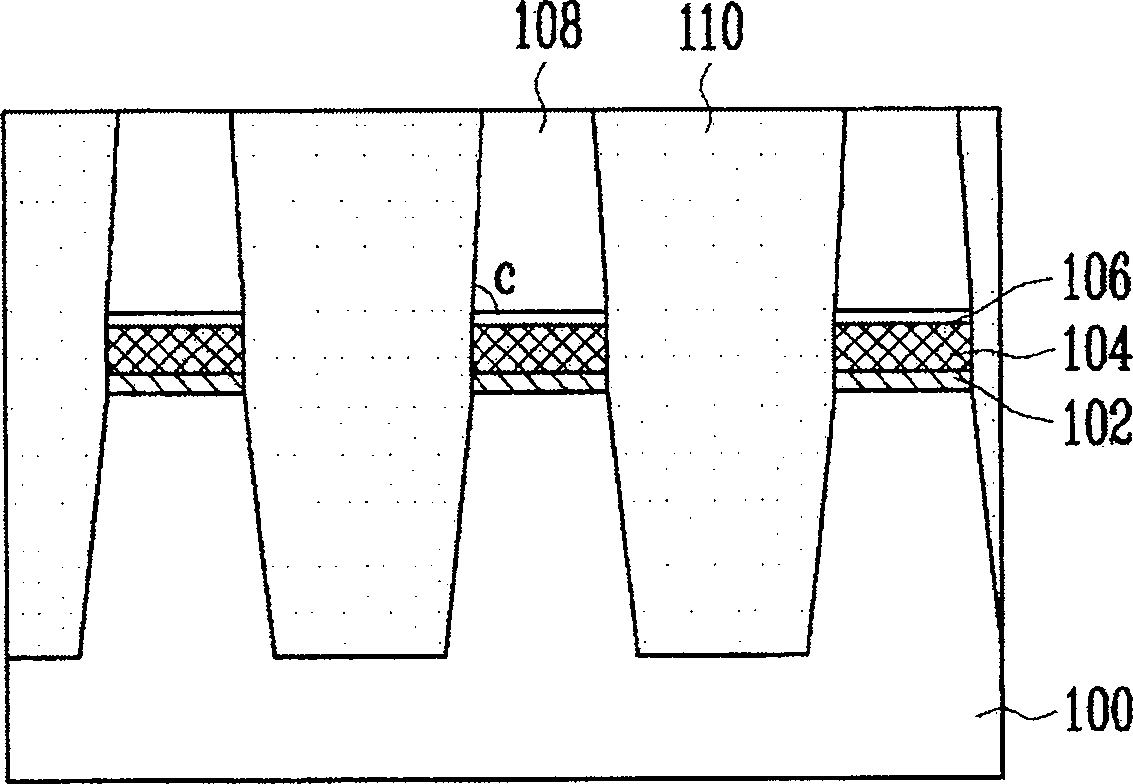
[0017] Figures 3A-3F is a cross-sectional view illustrating a method of manufacturing a NAND flash memory device according to an embodiment of the present invention. FIG. 3 shows a self-aligned shallow trench isolation (SA-STI) structure applying a self-aligned floating gate (SA-FG) scheme. refer to Figure 3A A channel oxide layer 102 , a first polysilicon layer 104 for a floating gate, a buffer oxide layer 106 and a nitride layer 108 are sequentially formed on a semiconductor substrate 100 . The first polysilicon layer 104 is preferably formed 300 -500 The thickness of the buffer oxide layer 106 is preferably formed 30 -80 thickness, the nitride layer 108 is preferably formed 600 -1200 thickness of.

[0018] Portions of the nitride layer 108, the buffer oxide layer 106, the first polysilicon layer 104, the channel oxide layer 102, and the semic...


PUM


Abstract

A method of manufacturing a NAND flash memory device, wherein isolation layers are formed in a semiconductor substrate and the upper side of each isolation layer has a negative profile. A polysilicon layer is formed on the entire surface. At the same time, a seam is formed in the polysilicon layer due to the negative profile. A post-annealing process is performed to void the seams. Accordingly, an electrical interference phenomenon between cells can be reduced and a threshold voltage (Vt) shift value can be reduced.

Description

technical field [0001] The present invention generally relates to a NAND flash storage device, and more specifically to a manufacturing method of a NAND flash storage device, wherein the electrical interference phenomenon between cells can be reduced by reducing the area of ​​the floating gate. Background technique [0002] In the manufacture of NAND flash memory, due to the improvement of device integration, the space size for forming a unit active region and a unit field region is reduced. For this, a dielectric layer and control gates and floating gates are formed in a narrow active space. Therefore, there is a problem of a crosstalk phenomenon due to the narrow interval between the gate electrodes. [0003] figure 1 is a perspective view illustrating a known common method of fabricating a NAND flash memory device using self-aligned shallow trench isolation (ST-STI). figure 1 The illustration shows the phenomenon of electrical interference between units. [0004] refe...

Claims


Application Information

Patent Timeline
Patent Type & Authority Patents(China)
IPC IPC(8): H01L21/8247H01L21/336
CPCH01L27/11521H01L27/115H10B69/00H10B41/30H10B41/35H01L21/31051
Inventor 李秉起
Owner SK HYNIX INC
Why Eureka
Try Eureka