

Semiconductor device having a frontside contact and vertical trench isolation and method of fabricating same
A trench isolation and semiconductor technology, applied in semiconductor/solid-state device manufacturing, semiconductor devices, electric solid-state devices, etc., can solve problems such as interfering with the performance of adjacent devices
- Summary
- Abstract
- Description
- Claims
- Application Information
AI Technical Summary
Problems solved by technology
Method used
Image

Examples
Embodiment Construction
[0035] The following reference Figure 4 , Figures 4a-4f and Figure 5 , to describe in detail the fabrication method of the device according to the exemplary embodiment of the present invention.
[0036] step 100
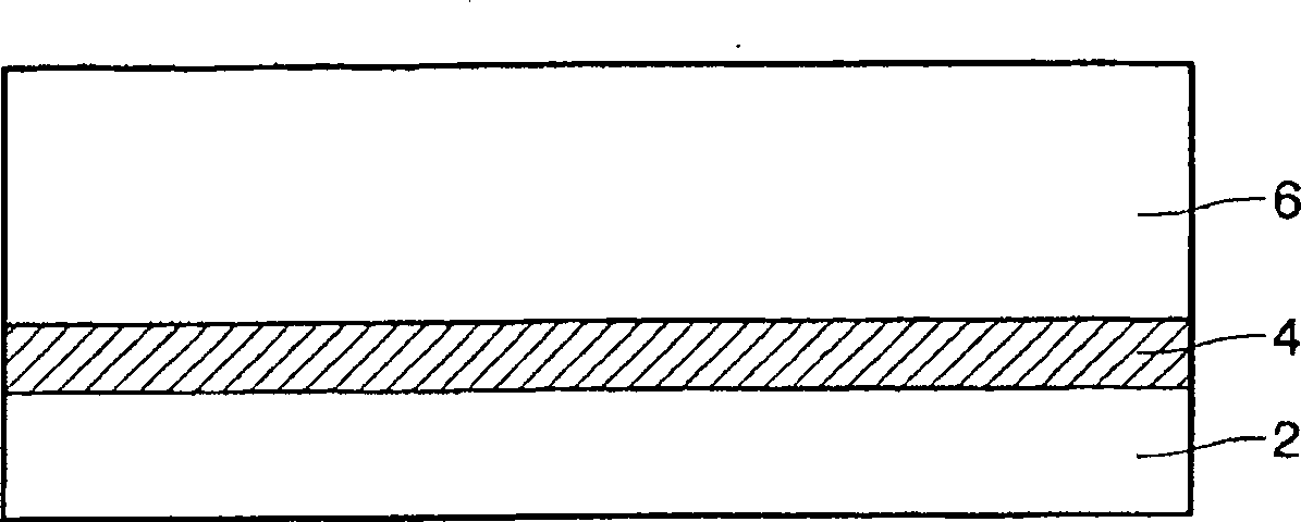
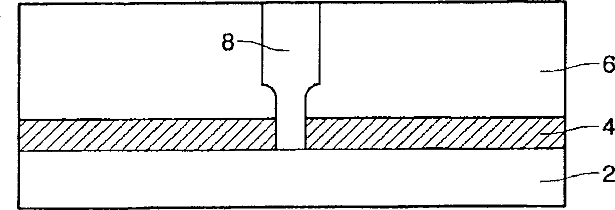
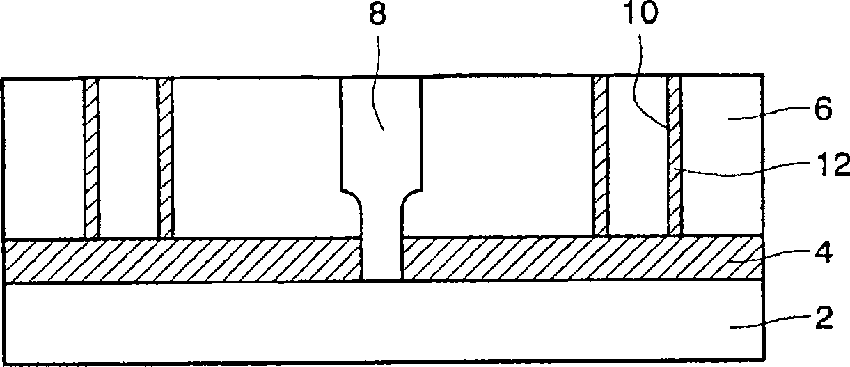
[0037] consider as Figure 4 A silicon-on-insulator substrate 20 is shown, wherein the bottom substrate layer 2 is composed of silicon, and the insulating layer 4 is composed of silicon dioxide (SiO 2 ) composition, and the active semiconductor layer 6 is composed of silicon. In the first step, a field-induced oxide layer is grown on the exposed surface of the active semiconductor layer 6 of the substrate 20 by an oxidation process, the layer comprising silicon dioxide (SiO 2 ) layer 22, the oxidation process is well known to those of ordinary skill in the art. The purpose of the field oxide layer is to protect the active layer 6 of the substrate 20 and to form doped carriers. A subsequent nitridation step may also be performed to form a nitride (Si 3 N 4...
PUM
 Abstract
Description
Claims
Application Information